The chips
The chips share one contract, and a lie about a pin fails the tests
nes-bus is the contract: the pin tables and frame types every chip speaks, in one small crate with no dependencies. It is more than something that compiles. A recorded run of the PPU (2c02) plays back through the contract’s pins, and we built in a sabotage that lies about one pin’s polarity, which the playback has to catch by failing.
The fifth chip matches its reference exactly, with no list of exceptions
2a03 is the NES CPU: a 6502 core, the clock divider and the audio units, all 10,946 transistors over 5,577 defined nodes, counted the same by two independent parsers. Its recorded run plays back against the reference simulator bit for bit across 601 states with no list of exceptions at all, the first of our chips to manage it. Getting there settled a question the engine had carried since its first release. At power-on the 2A03 has 3 groups of wires that the chip’s own layout pulls one way while something outside drives them the other, the first chip where that count is not zero, and halfphi 0.1.6 settles them the way the silicon does. We checked that the change makes no visible difference on any other chip.
First sound, and the note is exactly the program's
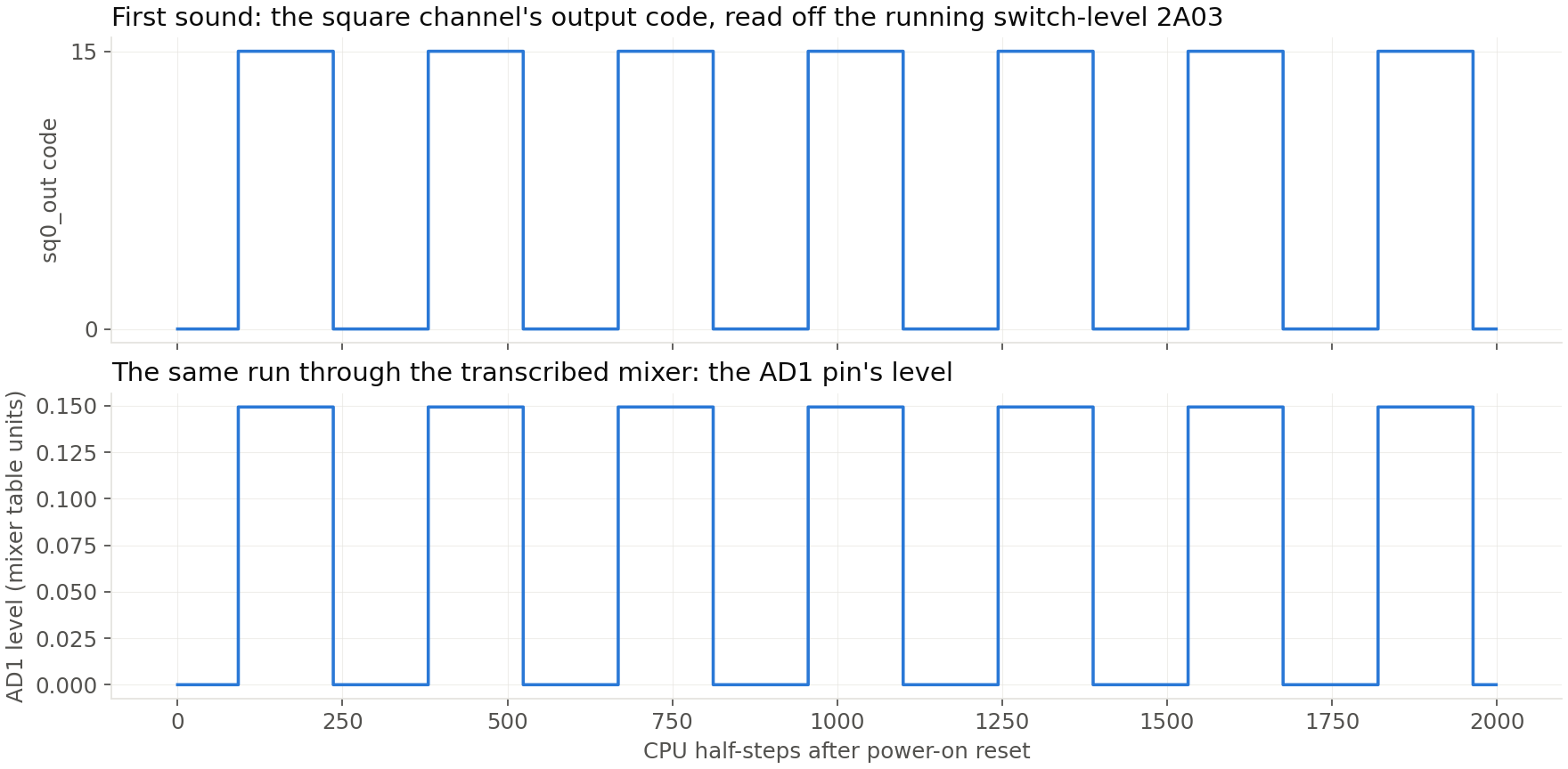
A small program of ours runs on the chip, with a simple stand-in for the console’s memory around it, and makes the square channel sing. The reference simulator ran the same program, and our chip matches that recording bit for bit over 2,001 states, with the core, the audio units and the bus logic all in the one comparison. And we measured the note itself rather than assuming it: the channel’s output steps through plateaus of exactly 144 half-steps, ten of them counted, and 144 comes straight from the program’s own timer byte (8). To prove both checks can fail, the test sabotages itself by serving that byte wrong. Both go red: the playback at the moment the byte first crosses the bus, and the plateau count at exactly the number the wrong byte predicts.
The PPU's disputed corners, each settled by a program written for it
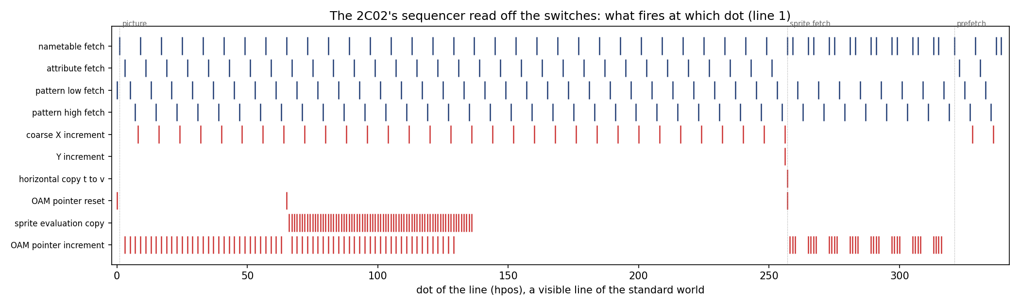
Emulator authors have argued for years about a few corners of the PPU. We answered each one with a short program of register writes run on the switch-level PPU (2c02), while the reference simulator ran the same program without knowing what we expected and recorded every node in the moments that matter. Sprite 0 hits at line 91, dot 182: the sprite’s own x plus the two dots the pipeline adds. Across both sprite tests our chip matches the reference node for node over 600 states, with no exceptions. The famous window in which a program can miss the vblank flag measures about a dot and a half wide. Three reads across the moment the flag rises return bit 7 as [0, 0, 1] (miss, suppress, consume), and the reference’s own recorded data bit agrees. Sprite memory (OAM) showed no corruption under either of the documented triggers.
Two engine divergences, both found by the chips and fixed in the engine
Getting sprite 0 to hit at all exposed the first. The reference treats a group of wires specially when it touches both power rails, and on the sprite memory’s data lines our engine had been crushing that case to zero. halfphi 0.1.5 fixes it the reference’s way, by holding the old value and letting the members’ areas vote on the charge. The second hid until we paced a palette write the way a real CPU paces it: on our engine the byte landed ORed with the low byte of the address, and on the reference it landed as written. The cause was how a group of wires that nothing drives settles. The 2C02’s reference weighs the members by area; visual6502 lets any one charged member win. halfphi 0.1.6 lets a netlist declare which rule it wants, and with the area vote declared, both of the PPU’s recorded reference runs play back with no exceptions at all: 601 states from power-on and 4008 states through the bus test rig, every one of 10,906 nodes. The 9 and then 27 latches those runs had set aside as unknown power-on state were the charge rule all along, not the silicon. A test now checks the declaration, and building the chip under the old rule turns it red.
The fast PPU matches the chip dot for dot, well inside the frame period
The fast PPU is not a second model of the chip. Its schedule is a table measured out of the switch-level chip when it is built, one entry per dot of a frame: which fetch the chip latched, when it stepped its address, when it copied the scroll, when the flag rose. Only the datapath is written by hand, and it is checked against the chip’s own frames. On the first test scene, 62160 visible dots agree with the switch-level render. On a scene of 64 sprites (flips, priority, nine on one line) all 61440 agree, with the sprite-0 hit landing at (92, 183) where the chip’s own flag rose at dot 185. On a scrolled scene with five register writes landing mid-frame, all 61440 agree, and each write takes effect inside its bus access (a plateau at dots 1, 2, 3 after the access starts). It renders a frame in 1.083 ms against the 16.639 ms frame period, 15.4 times inside it, worst frame 1.903 ms, over 200 frames.
The 2A03's core at the 6502's pins, chip against chip
The console sketch asks for a new kind of check, one chip against another through the contract, and both halves now exist. We present the 2A03’s 6502 core in the 6502 project’s own pin frames, one per clock phase, and run it through every recorded pin trace the 6502 has (289 of them: seven programs, the reference’s program, the scripted interrupt and RDY runs, three decimal-mode chains, all 256 opcodes). The 6502 takes part only as recorded text, never as a running engine. 285 traces compare (4 more drive pins the 2A03 does not have, and are refused by name), 131 of them exact in every field at every half-cycle. The rest differ only in four named, bounded ways. The stack page: the two dies’ simulated power-on stack pointers differ by $40, which we derived from both cores’ own registers. The data byte in the first half of a write, where nothing reads it. The decimal chains, where the 2A03 stores the plain binary sums and flags that the 6502 adjusts (9 bytes, listed with their arithmetic). And a reset in the middle of a run, where the 2A03 holds its core still while the 6502 carries on, and both read the vector on the same half-cycle. That list decided the shape of the 2A03’s own fast core: the 6502’s fast core with its decimal adjust switched off and its stack pointer seeded from this chip. Those two switches went into the 6502 repository, where they are checked against its recorded runs. Against the switch-level 2A03 on every program and script (285 programs, 65561 half-cycles), the only difference left is that byte in the first half of a write.
The sound unit as tables, matching the chip at every half-step
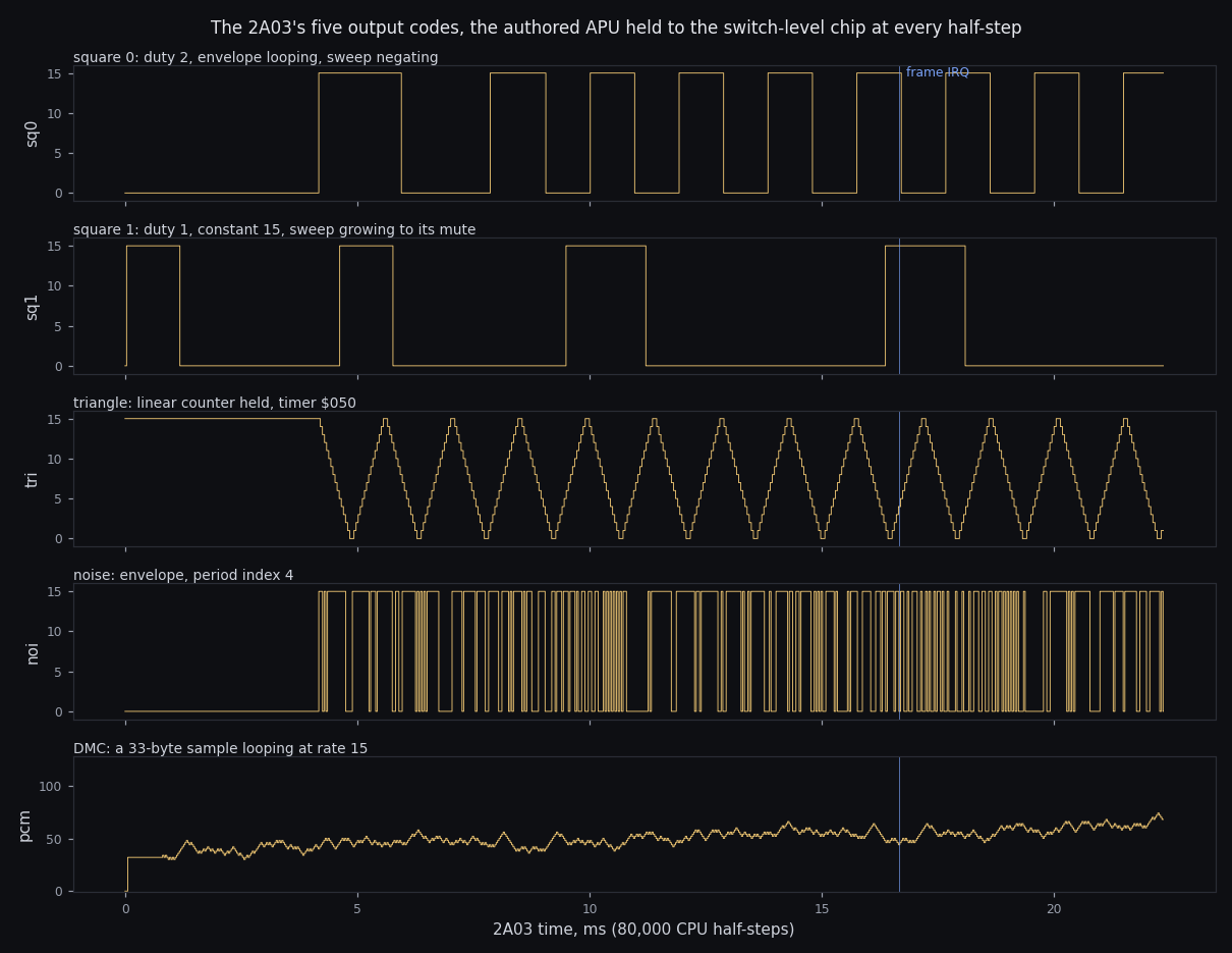
The sound side follows the PPU’s pattern: tables measured out of the switch-level chip at build time, the machinery around them written by hand from what small experiments showed, and the whole thing checked against the chip’s own output. The experiments came first, eleven measurements we kept as instruments (the frame sequencer in both modes, the length table, the duty sequences, the envelope and sweep clocks, the triangle, the noise and DMC period tables, the sprite DMA, the controller strobes), and they found two things the published model does not say. The noise and DMC timers are not counters but linear feedback shift registers. They run free from power-on, and each reloads one of sixteen recorded states when it reaches its end: those states are the die’s period ROMs. The noise ROM’s index 12 lands at 964 cycles where every published table says 762, which is either a transcription error in the die data or a real quirk of the part; we name it and carry it. Every timing inside a unit is a constant we measured the first time our version and the chip disagreed: a write to a period’s low byte makes the next tick a reload, a square’s output lags its step by two half-steps, and the DMC’s output counts eight completions from power-on before it makes a sound. The check runs two register programs under both frame modes, 10 test scenes of 80001 half-steps each, and the five output codes and the frame IRQ flag match the switch-level chip at every half-step. Then the stalls, where the chip’s DMA units take over the bus: the whole chip at its pins against the switch-level chip, frame for frame, with RDY compared like any other signal. A sprite DMA at both write alignments (1201 frames each, RDY low on 1029 and 1027) and the DMC’s sample fetches (4201 frames, RDY low on 19). With everything attached the chip runs at 32,067,032 half-cycles a second, 9.0 times real time. The step-by-step account is the N3 report.
Every number here comes from re-running the tests
The figures below come from running both chip repositories’ own test suites again on 2026-09-29, with their netlists and every recorded reference run required, plus the runs where we break things on purpose to make sure the tests notice, all at the recorded commits. This page reads only what those runs wrote.
The chips
The contract every chip speaks, then the NES's two chips at their switches (the 2A03 CPU and sound, the 2C02 picture chip) and the fast versions built from them.
- The contract the chips share N0 report: The pin tables, the dot frame and the cartridge edge as one small crate with no dependencies, checked against the recorded reference runs.
- The 2A03 at its switches, matching its reference exactly A0 report: The NES's CPU and sound chip simulated transistor by transistor, bit for bit against its reference with no list of exceptions.
- First sound from the 2A03 A3 report: A program's note read off the chip's own output, and the mixer written down as a claim we have not yet measured.
- Planning the fast 2A03 N3 plan: The 6502's fast core with its decimal adjust switched off, and the sound unit as tables measured out of the chip.
- The fast 2A03, built and checked N3 report: The fast chip checked at its pins against the transistor-level one, the sound tables measured out of the chip, and the bus stalls frame for frame.
- The 2C02 at its switches P0 report: The picture chip simulated transistor by transistor, its reference run replayed, and the transistors that only work when the supply is on found.
- The 2C02's first picture P1 report: The picture chip driven through its simulated bus, its colour output matching the table, and the latches that power up unset named.
- The 2C02's hard corners P2 report: Sprite 0, the vblank read race and OAM corruption, each settled by a small register program that the reference runs too, without knowing the answer.
- Planning the fast 2C02 P3 plan: A picture chip that steps one dot at a time, driven by a schedule measured out of the transistor-level chip.
- The fast 2C02, dot for dot with the chip P3 report: The fast picture chip agreeing with the transistor-level one on three test scenes, the register writes, and the picture with rendering switched off.
The repositories are public: github.com/tinymachines/2a03 and its siblings. The chip crates embed die data derived from visual6502-family imagery, so NonCommercial and ShareAlike travel with them; the contract crate is MIT and embeds nothing.