ブリッジの回路図と部品
印刷用: 図面一式「NES controller-port bridge, v1b」TM-NESB-001 版 P (PDF、英語)、組み上がった v1b、写真の上に検査箇所を書き出したもの (PNG)、図面一式「NES controller-port bridge, v2b」TM-NESB-002 版 A (PDF、英語)。
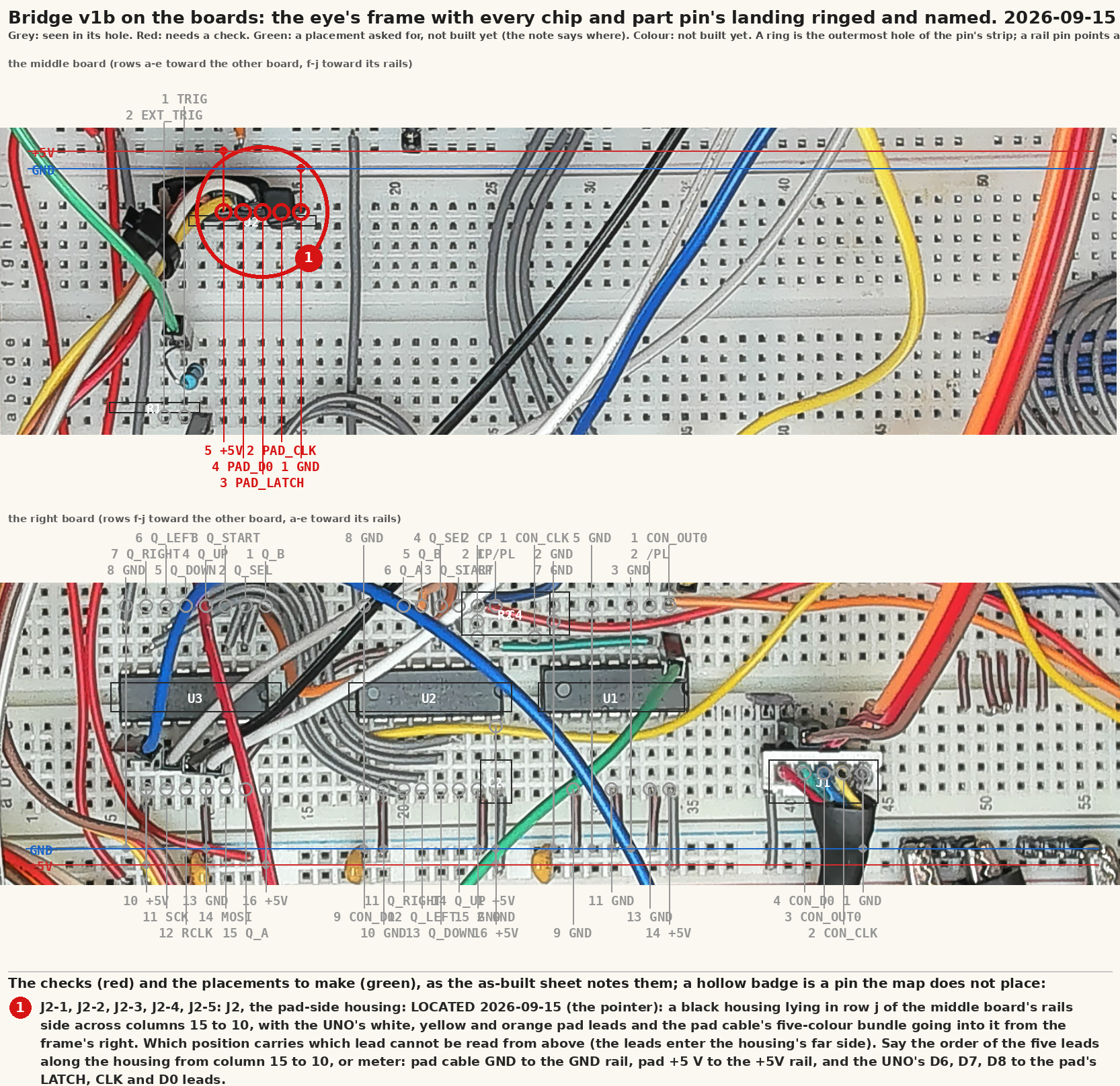
2026-09-07 に nes-bench の main (docs/wiring.md は 2026-09-07 改訂、
firmware/bridge/bridge.ino、head/headd.py) に対して、ベンチの電子回路
レビューから起こし、同じ日にリポジトリへ入れた。この文書には図面が 8 枚
付いている。うち 7 枚は tools/draw-schematics.py が、ヘッドの配線は
tools/wiring-diagram.py が生成するので、表が変わった後に作り直せる。
tools/check-sheets.py は v1 シートの C6 のピンを一つ残らず docs/wiring.md
に、v1b シートの UNO のピンを一つ残らず docs/bench-v1b-uno.md に、
コミット済みの SVG を生成器に押さえるので、シートとその表が離れていくことは
ない。
まず v1b を組む。 届いた 74HC の部品は 5 V で 3.5 V の高レベルを要求し、
C6 の 3.3 V ではそれが出ない。UNO は 5 V の部品で、レベルシフタを全部
不要にする。docs/bench-v1b-uno.md がその文書で、firmware/bridge-uno/ が
そのスケッチだ。下の v1 は C6 版として一式の中に残る。v2 のカウンタがそれを
必要とするときのために。
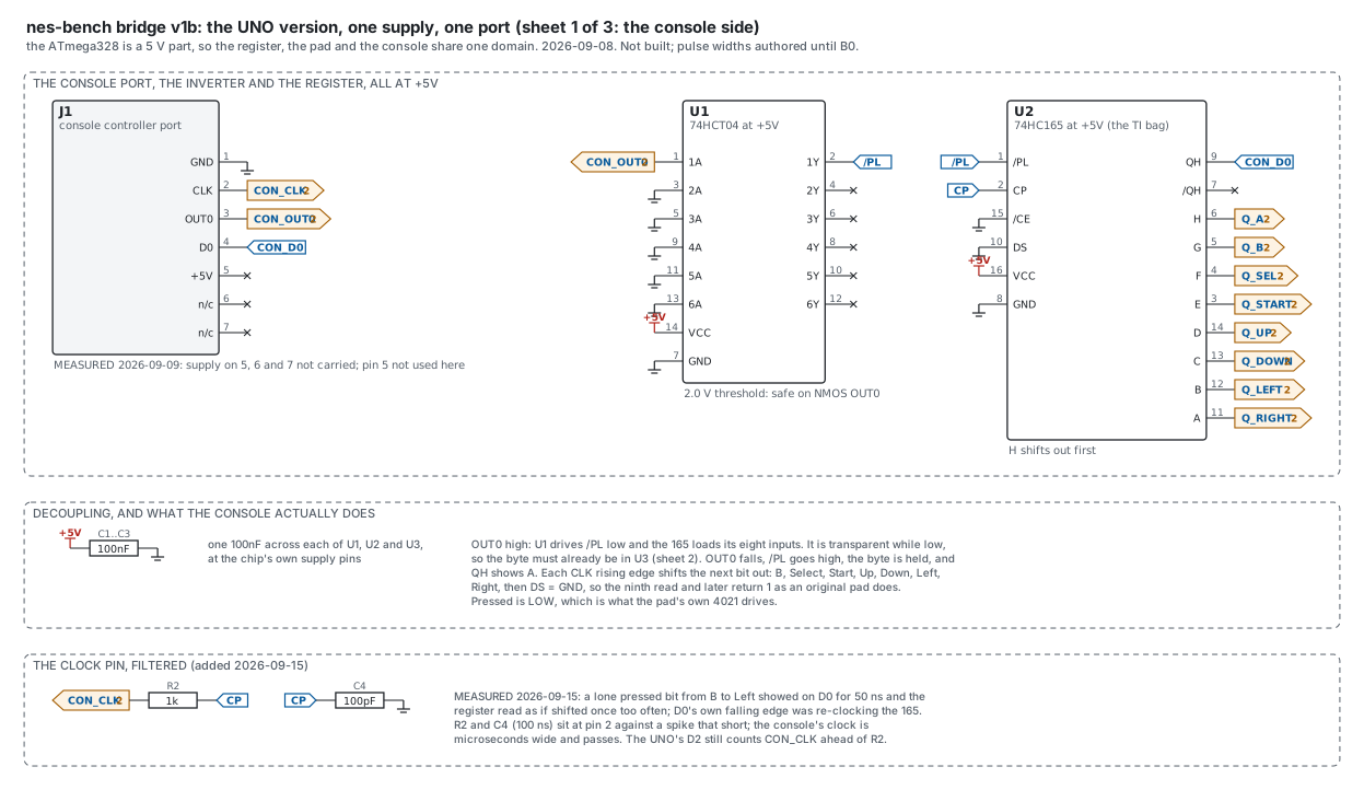
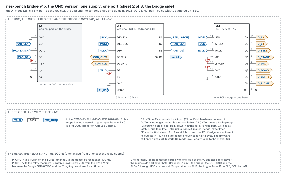
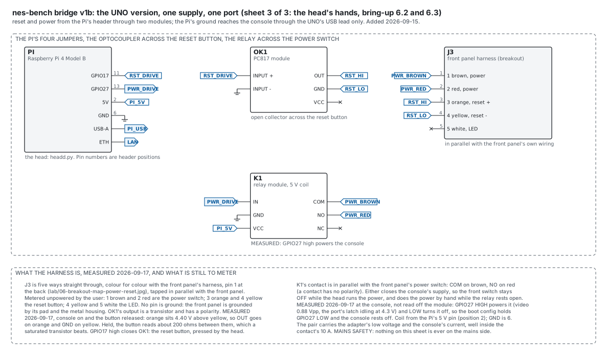
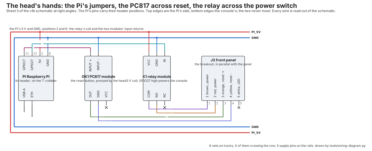
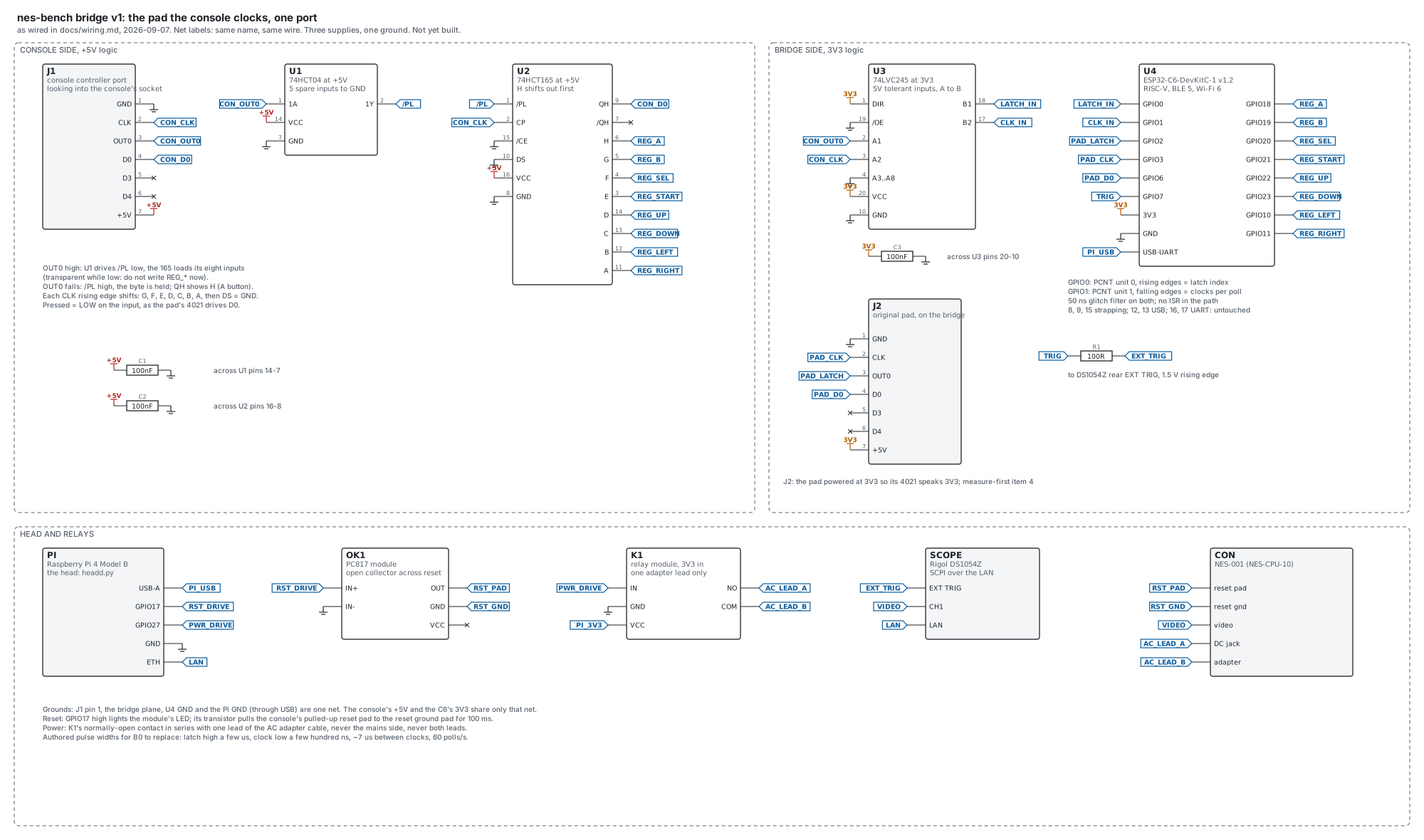
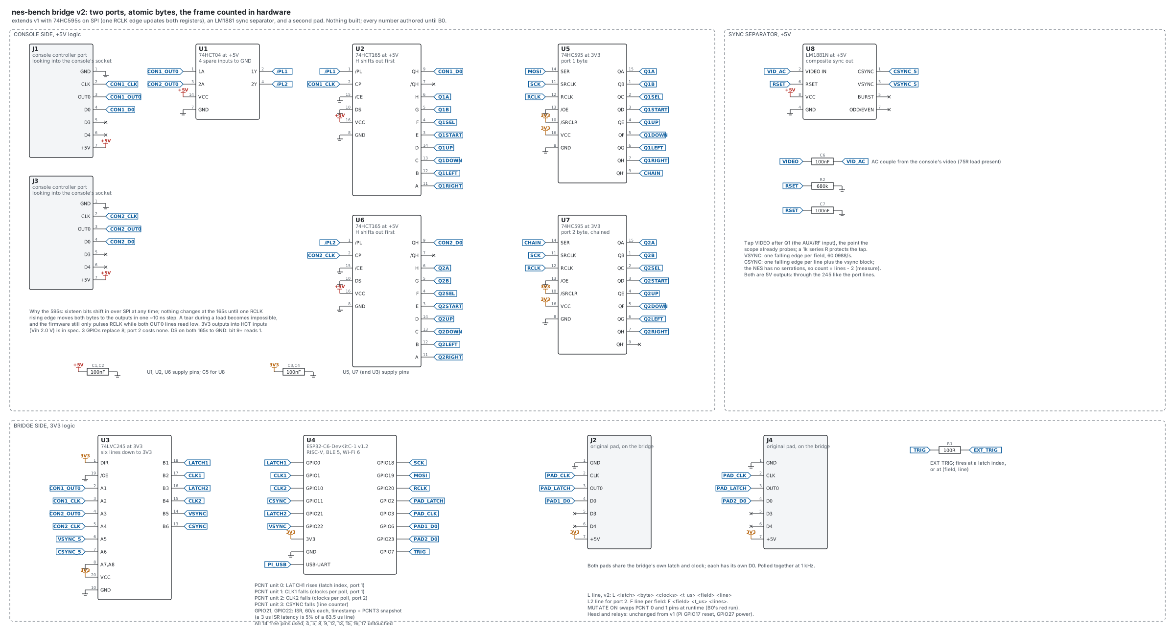
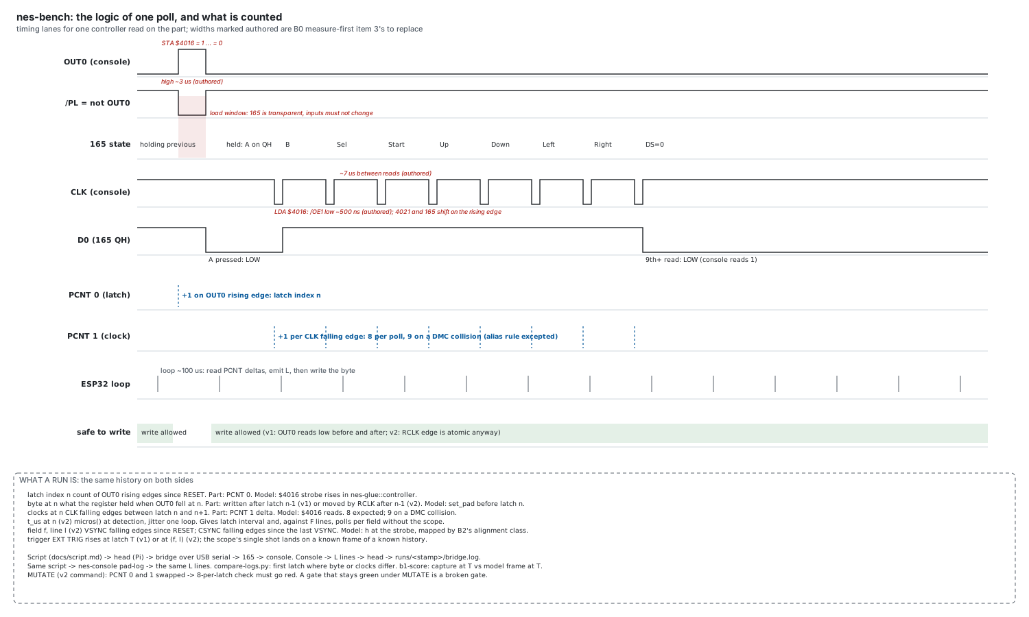
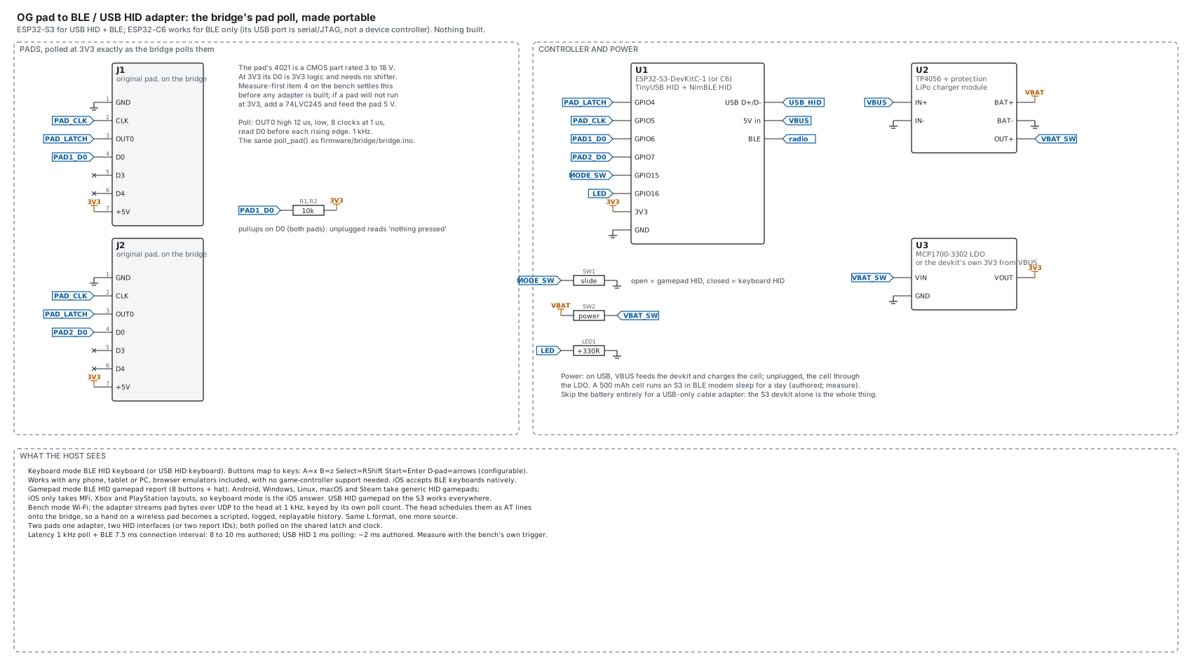
bench-v1b-1.svg、bench-v1b-2.svg、bench-v1b-3.svg: 同じブリッジを Arduino UNO で、電源 1 系統、横向きレター 3 枚に。3 枚目はヘッドの手 (Pi からのリセットと電源、立ち上げの 6.2 と 6.3)。74LVC245 も LS245 の 上げシフタも無い: UNO がコンソールの OUT0 と CLK を直接読み、595 を 5 V で 駆動する。wiring-v1b-head.svg: ヘッドの手を直角の配線として、Pi のジャンパをその ヘッダ位置で。3 枚目と同じネットリストから、tools/wiring-diagram.pyが 描く。bench-v1.svg:wiring.mdが言うままのブリッジ。ポート 1 個、レジスタへ GPIO 8 本、Pi の上に PC817 とリレー。bench-v2.svg: 拡張したブリッジ。ポート 2 個、レジスタは 74HC595 から SPI で供給されるのでバイトが 1 エッジで変わる。LM1881 の同期分離が付くので、 どのラッチもフィールド番号とライン番号を運ぶ。logical-timing.svg: 実機での 1 回のコントローラ読み出しをタイミングの帯に。 ロード窓、各カウンタが何を数えるか、両側でランとは何か、そして書き込みが 安全な場所。pad-adapter.svg: 純正パッドを電話向けの BLE か USB HID へ。ヘッドに 流し込むベンチモード付き。
作り直しは python3 tools/draw-schematics.py docs/ (Python 3、依存無し)。
ラスタライズは cairosvg か rsvg-convert で。PNG はコミットしない。
どの図面でも共通の取り決め: ネットラベルの回路図 (同じ名前なら同じ配線)、
電源はそれぞれレール記号で、その下に共通のグランド 1 本、レジスタでは
押下 = LOW。v1b は組んである (2026-09-15、bench-v1b-uno.md)。v1、v2 と
アダプタのシートは図面だ。タイミングの幅はどれも書き下ろしで、B0 の
「まず測る」項目 3 がそれを置き換えるまでそのままだ。シートは数字が出るところでそう書いている。
1. v1: wiring.md にあるものを、回路図として描く
v1 のシートは配線の文書に何も足さない。同じピン表を回路図の形にしたもので、 表では隠れる二つのことが見えるようにしてある:
- 165 のロード窓。/PL は OUT0 が高い間ずっと低く、その間レジスタは透過に
なる。
logical-timingのシートがそこに影を付けている。この窓の中で REG_A..REG_RIGHT に書くと、半分が古く半分が新しい状態でラッチされうる。 ファームウェアレビューの修正 (8 本を 1 回のポート書き込みで、しかも OUT0 が前後ともに低く読めるときだけ書く) は v1 のファームウェアの変更で、 ハードウェアは要らず、いまのbridge.inoに入っている: GPIO の出力 レジスタへの 1 回のストア、OUT0 が前後ともに低いことを条件に、そうでなければ 次のループへ先送り (STATUSが先送りの回数を数える)。ループはカウンタを 読み、書く前にラッチをログする。そしてMUTATE ONは二つのカウンタを 互いの線に付け替えるので、B0 の妨害はスクリプト 1 行になる。 - 三つの電源ドメインを三つのレール記号として。J1 の 5 番ピンから来る +5V
(2026-09-09 に実測。ピン配置は
wiring.mdの表だ) は U1 と U2 だけに 供給する。C6 から来る 3V3 は U3 とパッドへ。Pi は USB 経由で C6 に供給する。 三つすべてを跨ぐネットは GND だけだ。
v1 の部品
| 数量 | 部品 | 手元にある | 備考 |
|---|---|---|---|
| 1 | ESP32-C6-DevKitC-1 v1.2 | あり | U4 |
| 1 | Raspberry Pi 4 Model B | あり | ヘッド |
| 1 | 74HCT165 DIP-16 | U2、+5V で | |
| 1 | 74HCT04 DIP-14 | U1、1 ゲートだけ使う | |
| 1 | 74LVC245 (DIP か、ブレイクアウト上の SOIC) | U3、3V3 で | |
| 1 | PC817 フォトカプラモジュール | あり | OK1 |
| 1 | リレーモジュール、3V3 論理入力、接点はアダプタの電流より上の定格 | K1、VCC は Pi の 3V3 ピンから | |
| 3 | 100 nF セラミック | C1..C3 | |
| 1 | 100 R | R1、トリガ | |
| 1 | BNC から片側開放のケーブル、またはプローブ | トリガを CH1 へ | |
| 1 | コントローラのハーネスヘッダ用のブレイクアウトか圧着ピン | J1 | |
| 1 | ハーネス付きの 2 個目のコントローラポートのハウジング (コンソール自身のもの) | あり | J2 |
| ブレッドボードかユニバーサル基板、22 AWG の線、C6 と Pi をつなぐ USB-C ケーブル |
v1 の組み立て順
5 V のものが、測られる前に C6 に出会うことが決してないように選んだ順だ。
- テスタ、コンソール電源オフ。 ハーネスの各線から、基板ヘッダのポート
ピンまでの導通。色の対応表は
bench.local.mdに書く。色は証拠ではない。 - テスタ、コンソール電源オン、何も差さない。 ポートの 5 番ピンから 1 番 ピンで 5 V と読める。2 番はアイドルで高く、3 番はアイドルで低い。4 番は 高い (40H368 を通して R14/R15 でプルアップされている)。
- スコープ、もう一方のポートに純正パッド、ゲームを走らせて。 ラッチの パルス幅、クロックのパルス幅、1 回のポーリングあたりのクロック数、D0 の アイドル時と押下時のレベル。この 4 つの数字が、タイミングシートの 「書き下ろし」をすべて置き換える。
- コンソール側だけを組む: U1、U2、C1、C2 を基板に載せ、J1 の +5V から 電源を取り、他は何もつながない。U2 の H..A 入力をワイヤリンクで既知の パターンに固定し (たとえば A と Start を低、残りを高)、ゲームがポートを ポーリングしている間スコープで QH を見る。ラッチごとにパッドの順で 8 ビットが現れ、その後 LOW になる。これが「まず測る」項目 6 で、C6 が存在する 前に U1 と U2 を証明する。
- ブリッジ側だけを組む: U3、C3、C6、J2。C6 の電源は Pi から取る。J2 に
パッドを差す。シリアル越しの
STATUSが、ボタンに追従するパッドのバイト (pad_byte) を見せる。これが「まず測る」項目 4 で、4021 が 3V3 で動くのか を決める。 - 両側をつなぐ。 C6 からの REG_* を U2 の入力へ (手順 4 のワイヤリンクは
外す)、CON_OUT0 と CON_CLK を U3 へ、両方のプレーンの間に GND。コンソール
電源オン、
MODE PASS、ゲーム: L のストリームが現れ、ラッチごとに 8 クロック。それが B0 の最初の検査だ。 - トリガ。 R1 をスコープの CH1 へ。DS1054Z に外部トリガ入力は無い
(2026-09-15 に実測。ソース EXT は拒まれる)。
TRIG 300でスコープの シングルショットが発火する。水平オフセットの符号はここで決め、 キャプチャの.tomlに書く。 - リセット。 リセットボタンの二つのパッドをテスタで測る (どちらが
グランドで、もう一方は何ボルトに座っているか)。OK1 の OUT をプルアップ
されたパッドへ、GND をグランドのパッドへ、IN+ を Pi の GPIO17 へ。
スクリプトの中の
RESETがコンソールをラッチ 0 に落とし、L のストリームが 再開する。 - 電源。 K1 をアダプタケーブルの片方の線に直列に。決して交流側には
入れない。スクリプトの中で
POWER OFF/POWER ON。
2. v2: 拡張したブリッジ
変更は三つ。それぞれ独立で、それぞれレビューが挙げた理由がある。
2a. 各 165 の前に 74HC595
16 ビットが、連結した 2 個の 595 へ SPI でいつでもシフトインされる。165 の側 は、RCLK の立ち上がり 1 回が両方のバイトを 595 の出力へ 1 段で移すまで、何も 見ない。ロード中のちぎれは、起こりにくいどころか不可能になり、ファームウェア の「OUT0 が低い間だけ書く」検査は念のための二重の備えとして残る。GPIO 3 本 (SCK、MOSI、RCLK) が 8 本を置き換え、2 個目のポートはピンを 1 本も食わない。
595 は C6 からの 3V3 で走り、HCT165 の入力を直接駆動する: HCT の Vih は 2.0 V なので、3V3 の高レベルはきれいな高だ。/OE を GND へ、/SRCLR を 3V3 へ。
2b. 2 個目のポート
J3 はコンソールのもう一方のポートヘッダに、U6 は 2 個目の 165、/PL2 には U1 の
2 個目のゲート、CON2_OUT0 と CON2_CLK には U3 の A3/A4。2 個目のパッド J4 は
ブリッジ自身の PAD_LATCH と PAD_CLK を J2 と共有し、自分の D0 を持つ。二人
プレイの履歴は、AT と AT2 の行を持つ 1 本のスクリプトと、L と L2 の
行を持つ 1 本のログになる。
2c. LM1881 同期分離
コンソールのコンポジット映像を +5V の LM1881 に AC 結合で入れると、きれいな VSYNC と CSYNC の出力が得られる。U3 を通して C6 へ:
- VSYNC は GPIO 割り込みへ (毎秒 60 回): フィールドのカウンタ。タイムスタンプ と、ラインカウンタのスナップショットを添えて。
- CSYNC は PCNT のユニット 3 へ: ラインのカウンタ。NES はセレーションパルスを 出さないので、1 フィールドあたりの計数はライン数から小さな定数を引いた値に なる。一度測り、記録し、それを使う。
こうすると L の各行が <field> <line> を運ぶ。フレームの中でそのポーリングが
どこにいたかを、ハードウェアで測った値で。模型はそれをストローブ時の h として
知っていて、B2 の整列クラスが両者を対応させる。B0 の「1 フレームあたりの
ポーリング数」の検査は、スコープなしでブリッジの内側で閉じる。
v2 の C6 でのピン予算
空いているピンは 14 本。全部使う:
| C6 のピン | 役割 | ペリフェラル |
|---|---|---|
| GPIO0 | LATCH1 (CON1_OUT0 の立ち上がり) | PCNT 0 |
| GPIO1 | CLK1 (CON1_CLK の立ち下がり) | PCNT 1 |
| GPIO10 | CLK2 | PCNT 2 |
| GPIO11 | CSYNC の立ち下がり | PCNT 3 |
| GPIO21 | LATCH2 | GPIO ISR |
| GPIO22 | VSYNC | GPIO ISR |
| GPIO18, 19, 20 | SCK, MOSI, RCLK | SPI2 |
| GPIO2, 3 | PAD_LATCH, PAD_CLK (両方のパッドで共有) | GPIO 出力 |
| GPIO6, 23 | PAD1_D0, PAD2_D0 | GPIO 入力 |
| GPIO7 | TRIG | GPIO 出力 |
LATCH2 を PCNT のユニットではなく割り込みに置くのが妥協点だ: C6 のユニットは 4 個しかない。ラッチは毎秒 60 回で、3 µs の ISR レイテンシはタイムスタンプの ジッタで走査線 1 本の 5% にあたる。ポート 2 にはそれで十分で、そう書いておく。 ポート 1 はハードウェアのカウンタを保つ。
v2 の部品、v1 からの差分
| 数量 | 部品 | 備考 |
|---|---|---|
| 1 | 74HCT165 | U6、ポート 2 |
| 2 | 74HC595 DIP-16 | U5、U7、3V3 で |
| 1 | LM1881N DIP-8 | U8、+5V で |
| 1 | 680 k | R2、LM1881 の RSET |
| 2 | 100 nF | C6 (映像の結合)、C7 (RSET) |
| 1 | 1 k | 映像タップの直列保護 |
| 4 | 100 nF | U5、U6、U7、U8 のデカップリング (チップ 7 個、コンデンサも全部で 7 個) |
| 1 | 2 個目のポートヘッダ用のブレイクアウト | J3 |
| 1 | コンソールのもう一方のポートのハウジングとハーネス | J4 |
v2 のファームウェア、差分
write_registerは 16 ビットの SPI 転送 1 回と RCLK のパルス 1 回になり、 両方の OUT0 の線が前後ともに低く読めることを条件にする。- PCNT のユニット 2 と 3。
micros()と PCNT 3 の計数を保存する GPIO ISR が 2 本。 L n hh c t_us f l、L2 ...、F f t_us lines。AT2 n hh、TRIG nは変更なし、TRIGF f lを新設。MUTATE ON|OFF: PCNT 0 と 1 を互いの GPIO に再設定する。「ラッチあたり 8 個」の検査は、これを入れたら赤にならなければならない: B0 の妨害を、 スクリプトで。- ループの順序: カウンタを読み、行を出し、それから書く。
Stringではなく 固定長の行バッファ。スケジュールは走査するのではなくカーソルで。
3. Raspberry Pi の役目
Pi がヘッドだ。ベンチで唯一の常時稼働の Linux 機で、C6 にできない四つのことを やる (組んだベンチでは UNO が C6 の場所にいて、分担は同じだ):
- USB ホスト。 C6 は USB のデバイス側 (その UART ポート) だ。もう一方の 端に何かが居て、L のストリームを読みコマンドを書かねばならない。
- Ethernet と SCPI。 DS1054Z は LAN 上の生の TCP ソケットで駆動する。
1200 万点のキャプチャは 12 MB で、ヘッドがそれを分割して読み、
.u8と.tomlを書き、走行のディレクトリを HTTP で配る。C6 に Wi-Fi はあるが、 それを置くストレージが無い。 - リレー。 3V3 の GPIO 2 本 (17 が PC817 経由のリセット、27 が電源) で、 それらとコンソールの間の絶縁はモジュールが受け持つ。リレーを Pi に置いて おくと、5 V と交流に近い配線を C6 から完全に遠ざけられる。
- 指揮。
headd.pyが 1 本のスクリプトを 1 行ずつ演じ、head.logとbridge.logを保ち、トリガの前にスコープを待機させ、キャプチャを待ち、 systemd のサービスとして起き続ける。ワークステーションは走行の途中で 寝てよい。走行は終わる。
分け方はこうだ: C6 はマイクロ秒を持つ (ポーリングの合間にレジスタを書く、 エッジをハードウェアで数える、ラッチでトリガを上げる)。Pi は秒とメガバイト を持つ (スクリプト、リレー、SCPI、キャプチャ、HTTP)。どちらもナノ秒の経路 には居ない。そこは 165 のものだ。
C6 が Pi を置き換えられるか。リレーは駆動できるし、Wi-Fi で SCPI も話せる。 だがキャプチャは保持できず、USB ホストにもなれず、そうなると唯一のループが シリアルと TCP とタイミングを同時にやることになる。Pi は追加の費用がかからず (手元にある)、ファームウェアを考えられる大きさに保ってくれる。このままで いく。
4. パッドのアダプタ: 純正パッドから BLE か USB HID へ
組んだとおりのもの (2026-09-27)。 下の表のどちらの部品でもない。C6 は一度も
書き込みを受け付けず、基板は Waveshare の ESP32-P4-Module-DEV-KIT で、その上では
BLE が落ちる (モジュール搭載の C6 がホストスタックに応えない)。組んだのは USB だ:
P4 のフルスピードのコントローラ上の firmware/pad-usb、3.3 V の純正パッド、Linux の
ホストですべてのキー。下の組み立て順の手順 1 から 3 はそのやり方で済み、4 から 7 と
電話は開いたままだ。記録は pad-ble-build.md、基板の選択は esp32-part-choice.md、
プロトコルは pad-usb-protocol.md。2026-09-07 に書いた節がこの後に続く。
ブリッジはすでにアダプタを内に持っている。bridge.ino の poll_pad() が、
GPIO 3 本で 3V3 の本物のパッドをポーリングしている。アダプタとは、その関数の
後ろにシフトレジスタではなく無線が付いたものだ。
どの ESP32 か
| ESP32-C6 | ESP32-S3 | |
|---|---|---|
| BLE HID (キーボード、ゲームパッド) | 可、BLE 5 | 可 |
| USB HID | 不可: USB ポートはシリアル/JTAG のブリッジで、デバイスコントローラではない | 可、TinyUSB での USB OTG |
| Bluetooth Classic | 不可 | 不可 |
| Wi-Fi (ベンチモード) | 可 | 可 |
ケーブルとしても使えるべきアダプタには S3 が正しい部品だ: 開発キット 1 枚、
電池なしで、どんなホストにも USB HID のゲームパッドかキーボードとして。C6 は
BLE 専用のアダプタなら使えるし手元にあるので、S3 を発注する前に、ベンチの
ファームウェアの poll_pad と NimBLE の HID サービスで最初の試作を C6 で
作れる。
ホストに何が見えるか、そしてなぜ二つのモードか
- キーボードモード。 BLE (または USB) の HID キーボード。ボタンをキーに 割り当てる (A = x、B = z、Select = 右 shift、Start = enter、十字キー = 矢印。 設定可能)。電話もタブレットも PC もキーボードなら受け取るし、ブラウザの エミュレータはどれもキーを取る。iOS はペアリング用のアプリなしで BLE の キーボードを受け取る。電話のためのモードはこれだ。
- ゲームパッドモード。 HID のゲームパッドのレポート: ボタン 8 個とハット。 Android、Windows、Linux、macOS、Steam は汎用の HID ゲームパッドを受け取る。 iOS は MFi、Xbox、PlayStation、Switch Pro のレイアウトしか受け取らないので、 iOS ではゲームパッドモードは役に立たず、スイッチのところにそう書く。
- ベンチモード。 Wi-Fi でヘッドへ。パッドのバイトをポーリングのレートで
UDP に載せ、アダプタ自身のポーリング数で鍵付けする。ヘッドはそれを
ATの 行としてブリッジに予約するので、無線パッドに置いた手が、同じ L の形式の、 スクリプト化されログされ再生できる履歴になる。B3 のrecordにとっては 入力源が一つ増え、ベンチのトリガでアダプタ自身のレイテンシを測る道にも なる。
アダプタの部品
| 数量 | 部品 | 備考 |
|---|---|---|
| 1 | ESP32-S3-DevKitC-1 (BLE だけなら C6 でも) | U1 |
| 2 | ハーネス付きコントローラポートのハウジング、または 7 ピンの NES ソケット | J1、J2 |
| 2 | 10 k | D0 のプルアップ。差していないパッドが何も押されていないと読めるように |
| 1 | スライドスイッチ | モード |
| 1 | LED と 330 R | 状態表示 |
| 任意 | 保護付き TP4056 充電モジュール、500 mAh の LiPo、MCP1700-3302 の LDO、電源スイッチ | 電池版のみ |
ケーブル専用のアダプタなら、S3 の開発キット、ソケット 2 個、抵抗 2 本で全部だ。
アダプタの組み立て順
- まずベンチで「まず測る」項目 4: 3V3 の純正パッドがボタンに追従すること。 もし追従しないなら、アダプタには 74LVC245 とパッドへの 5 V が要り、シートに どこかが書いてある。2026-09-27 に完了: 追従する。245 は要らない。
- J1 を GPIO4、5、6 と 3V3/GND につなぐ。ベンチの
poll_padを焼いてバイトを 印字する。ボタンが現れる。2026-09-27 に完了、P4 の上で (B 01からB 80)。 - HID のサービスを足す (どちらのチップでも NimBLE、S3 なら TinyUSB)。まずは キーボードモード。電話ならアプリなしで動いているのが見えるからだ。 2026-09-27 に P4 の TinyUSB として完了。ホストはいまのところ電話ではなく Linux 機だ。
- スイッチの後ろにゲームパッドモード。
- 2 個目のソケットを GPIO7 に、ラッチとクロックは共有。
- ベンチモード: UDP の送信側と、
headd.pyのPAD要求。 - 電池は最後。ケーブル版が望まれていると分かったときだけ。
レイテンシは書き下ろしで、ベンチで測ることになる: 1 kHz のポーリングに 7.5 ms の BLE 接続間隔を足して 8 から 10 ms。USB HID の 1 ms ポーリングなら 約 2 ms。測り方は、アダプタのラッチ線に対するブリッジのトリガと、ホストの 最初のレポートを、スコープの上で突き合わせることだ。
5. シートで使う記法
- ネットフラグ (青いタグ): その配線の名前。同じ名前のピンはすべてつながっ
ている。
CON_*は 5 V のコンソール側。*_IN、LATCH*、CLK*は 245 を 通った後の同じ信号で 3V3。REG_*とQ*はレジスタの入力。PAD_*は ブリッジ自身のパッドの線。 - レールの記号: 赤いバーが
+5V(コンソール)、橙のバーが3V3(C6)、 グランドの記号がGND(唯一の共有ネット)。 - ピンの上の X: 未接続。
- ピン番号は DIP パッケージのもの。C6 のものは GPIO 番号。
- タイミングシートの赤い影: レジスタのロード窓、入力が変わってはいけない ところ。緑の影: 書き込みが安全なところ。青い破線の目盛り: PCNT の ユニットが数えるエッジ。
- 赤いイタリック: 書き下ろしの数字。測定を待っているもの。
6. 再確認で入れた訂正、2026-09-07
- v2 のシートで LM1881 の 5 番ピンと 7 番ピンが入れ替わっていた: 5 番はバースト /バックポーチの出力、7 番は奇数/偶数だ。どちらも未使用 (NC)。ラベルはいま データシートのものになっている。
- v1 のシートでリレーモジュールの VCC が C6 の 3V3 レールに描かれていた。実際
は Pi の 3V3 ピン (
PI_3V3) で、配線の文書がリレーを Pi に置くことでそう 示している。部品表にそう書いた。 - タイミングシートで書き下ろしていたラッチの高レベルの幅は約 2 us だったが、 二つの $4016 書き込みの間にある LDA/STA の対は CPU の約 6 サイクル、約 3.4 us なので、いまは約 3 us と読める。まだ書き下ろしだ。
- 組み立て順の手順 4 を書き直した。文の途中で自分と矛盾していた。
- v2 のデカップリングの数を訂正: チップ 7 個、100 nF も 7 個、うち新規が 4 個。
- iOS のゲームパッドの注記に、受け取るレイアウトとして Switch Pro を加えた。
draw-schematics.pyは、パスを埋め込む代わりに出力ディレクトリを引数で 取る。
出典に照らして変わっていないことを確認した項目: 74HCT165、74HC595、74LVC245、
74HCT04 のピン番号をそれぞれのデータシートに対して。v1 のネットと GPIO を
すべて docs/wiring.md に対して (165 の H..A は GPIO18..23、10、11。245 の
B1/B2 は GPIO0/1。パッドは GPIO2、3、6。TRIG は GPIO7。Pi の GPIO17 と 27)。
C6 の PCNT のユニットは 4 個で、v2 の予算はそれを使い切る。
ビルド時に nes-bench/docs/bench-build-v1-v2.md から取り込んだもので、リポジトリが唯一の写しだ。報告は独自の作業用の言葉をいくつか使う: 報告書で使われる言葉。