Arduino UNO の上の v1b ブリッジ
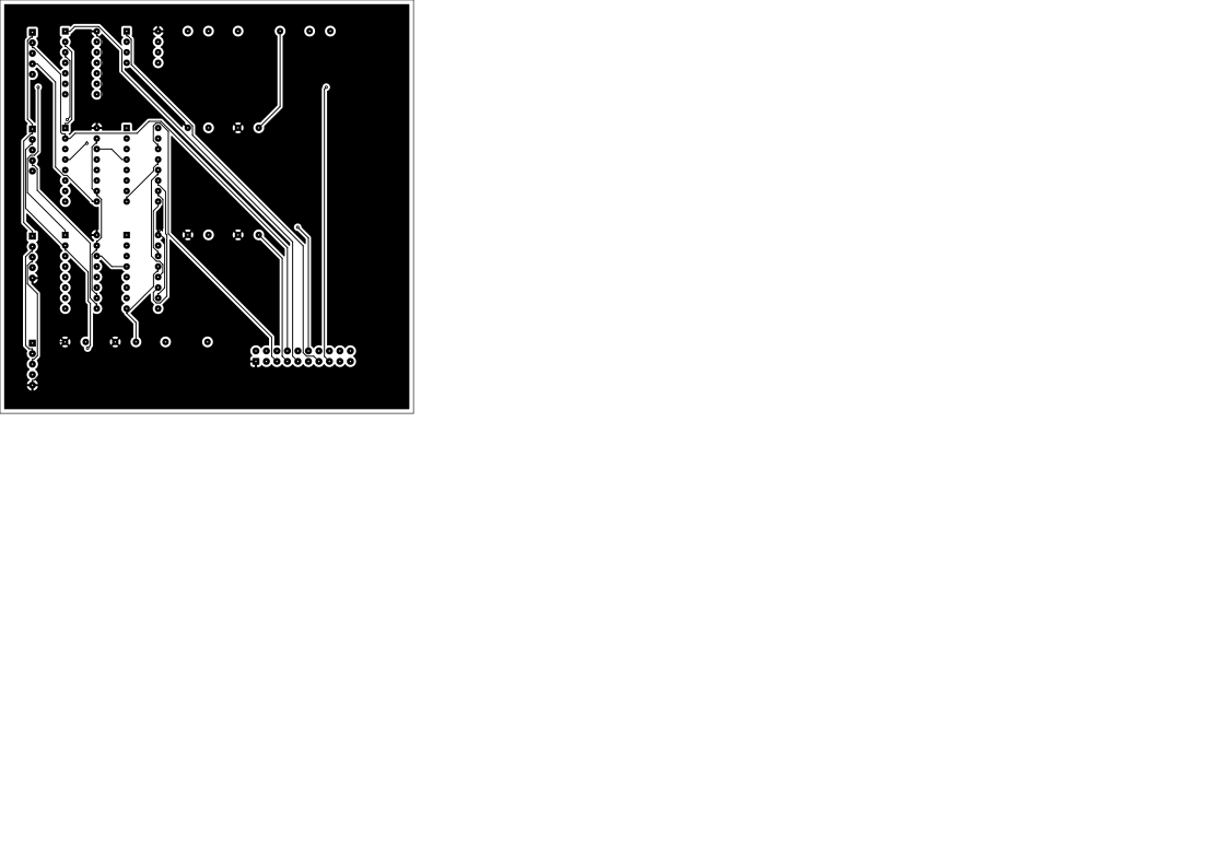
印刷用: 図面一式「NES controller-port bridge, v1b」TM-NESB-001 版 P (PDF、英語)、組み上がった v1b、写真の上に検査箇所を書き出したもの (PNG)、図面一式「NES controller-port bridge, v2b」TM-NESB-002 版 A (PDF、英語)、v2b 基板、表面の銅 (SVG)。
部品が届いた後、2026-09-08 に追加。最初に作るものとして v1 に取って代わる。v1 は、 v2 の計数器が要求するときのための C6 版として、一式の中に残る。
なぜ
届いた 74HC の部品 (HC165、HC595) は、5 V では 3.5 V の高を要求する。ESP32-C6 が 出すのは 3.3 V だ。UNO の ATmega328P は 5 V の部品なので、これを真ん中に置けば コンソール側の信号はすべて 5 V で規格の内に入り、三つのことが落ちてくる:
- 74LVC245 は無し: UNO がコンソールの OUT0 と CLK を直接読む。
- プルアップ付きの 74LS245 による昇圧も無し: UNO が 595 を 5 V で駆動する。
- パッドは、それが作られた 5 V でポーリングされる。まず測る項目の 4 (4021 は 3.3 V で動くか) は、もう何の門にもならない。
部品 (すべて手元にある)
| 記号 | 部品 | 出どころ |
|---|---|---|
| A1 | Arduino UNO R3 | 山の中 |
| U1 | SN74HCT04N | 2026-09-09 に届いた一本。HCT は入力しきい値 2.0 V で、2A03 の NMOS の OUT0 で安全 |
| U2 | SN74HC165N | TI の袋 |
| U3 | SN74HC595N | 30 個入りの箱 |
| C1..C3 | 100 nF | |
| R2 | 1 k、CON_CLK から U2 の CP へ | 手元にある。2026-09-15 からシートに載っている |
| C4 | 100 pF、CP から GND へ | 手元にある。2026-09-15 からシートに載っている |
| R1 | 100 R、スコープの CH1 へ入るトリガ (DS1054Z に EXT TRIG は無い。2026-09-15 に 2.5 V を実測) | |
| J1 | コンソールのポートのヘッダハーネス | |
| J2 | コンソールのもう一方のポートのハウジング | |
| DIP-14 と DIP-16 のソケット | キットの中 |
UNO のピン
| ピン | 機能 | なぜこのピンか |
|---|---|---|
| D13, D11 | U3 への SCK、MOSI | ハードウェア SPI、4 MHz、8 ビットを 2 us で |
| D10 | U3 への RCLK | 立ち上がり一つでバイトが動く。D5 が低を読んでいる間だけパルスする |
| D5 | CON_OUT0 | Timer1 の外部クロック入力 (T1): ラッチの立ち上がりを数える 16 ビットのハードウェア計数器。書き込みの門のためにレベルとしても読める |
| D2 | CON_CLK | INT0、立ち下がりの ISR: ポーリングあたりのクロック |
| D3 | TRIG | ラッチ T で立ち上がる。ループ一回ぶん遅れる |
| D6, D7, D8 | PAD_LATCH、PAD_CLK、PAD_D0 | ブリッジ自身のパッドのポーリング、5 V で |
| D0, D1 | UNO の USB を通した Pi へのシリアル | 115200 |
| 5V, GND | ブリッジの電源とグランド | USB を通して Pi から |
Timer1 を外部クロックのモードにすると、エッジは 16 MHz のクロックに同期して 数えられるので、数えられるにはパルスが CPU の 1 サイクル (62.5 ns) より長く なければならない。コンソールのラッチのパルスはマイクロ秒の単位だ。このピンには グリッチのフィルタは無い。L のストリームが、ポーリングあたり 1 でないラッチ数を もし見せたら、D5 に 100 pF をグランドへ足して、それを記録する。これは、シートが すでに持っているフィルタとは別のピンの話だ: R2 と C4 は 165 のクロックのピンに 座っていて、2026-09-15 に測ったスパイクに対するものである。
ファームウェア、bridge.ino からの差分
docs/script.md のプロトコルは変わらないので、headd.py と道具たちはシリアルの
速度以外に何も要らない。
write_register(b):SPI.transfer(~b)、そしてdigitalRead(5)が LOW なら、 D10 を 1 命令ぶん高にパルスして D5 をもう一度読む。パルスをまたいで HIGH に なっていたら、次の L の行に印を立てる。補数は見かけの問題ではない: レジスタでは 押された状態が LOW だ。SPI は MSB 先頭で、最初に送ったビットがいちばん遠くまで 進むので、ビット 7 を先に送ると私たちのビット 0 が QA に載る。それが A ボタンだ。 どちらかを逆にすれば、パッドは黙って鏡像になる。- ラッチの計数:
TCNT1(16 ビット) を読み、32 ビットの累計を持ち、巻き戻りを 処理する。クロックの計数: INT0 の ISR の中の volatile な計数器。 - ループの順序: 計数を読み、L を出し、それから書く。行バッファは 64 バイト固定で、
Stringは使わない。スケジュールはカーソルで、走査ではない。 - スケジュールが持てたのは 128 項目で、C6 の 2048 ではない。この部品の SRAM は
全部で 2 KB しかなく、権威はコンパイラだ: 256 にしたらグローバルが 2161 バイト、
105 パーセントと報告して、リンクを拒んだ。128 では 1521 と報告し、スタックに
527 を残した (2026-09-08 のビルド。2026-09-18 までには 1533 と 515、下の表)。
2026-09-19 以降は 600 を、詰めた形で持つ (下の節「ブリッジはどう
働くか」)。2026-10-18 以降、その 600 はヘッドが走行中に継ぎ足す輪になり、
記録はもうその数に縛られない (nes-bench 8f35ed6)。
tools/fake-bridge.pyは 同じ輪を真似るので、走行を予行できる。そしてヘッドは、ブリッジが# schedule fullか# lateと答えた走行をすべて止める。 - AVR のコアに
Serial.printfは無く、avr-libc の printf は 64 ビットの変換を 持たないので、C6 のuint64_tの計数器と%lluは、役に立たないものにコンパイル されていたはずだ。ここの計数器はどれもuint32_tと%luで、ラッチの添字は 毎秒 60 ポーリングなら 2.2 年で巻き戻る。 - L の行は 4 フィールドのまま、
L n hh c。タイムスタンプは v2 のt_usのもので、 ここには属さない:tools/b3.py、tools/compare-logs.py、head/headd.pyは どれもちょうど 4 つを要求するので、5 番目のフィールドは記録と比較とヘッドの ラッチ追跡を一度に壊す。ヘッドは受け取ったものに、すでにタイムスタンプを打って いる。 MUTATE ON: ジャンパも設定ピンも無い。D5 は PD5 であり、同時に PCINT21 でも あるので、Timer1 がハードウェアでそれを数え続けたまま、ラッチ線がピン変化の 割り込みを上げられる。MUTATE の下では、クロックの計数器はその割り込みの 立ち上がりだけで進み、INT0 はそれを進めるのをやめる。それが B0 が述べた妨害、 クロックの計数器をラッチ線から食わせるというもので、ソフトウェアだけでやるので 戻し忘れる部品が無い。妨害した走行はラッチあたり 8 ではなく 1 クロックを報告 するので、ラッチあたり 8 のゲートは赤になる。
ブリッジはどう働くか: UNO の仕事、そのコード、その下にある考え
この節は、Arduino がコンソールとパッドの間で実際に何をしているかを、要る所では
一行ずつ知りたい読者のためのものだ。スケッチは
firmware/bridge-uno/bridge-uno.ino で、そのスケジュールは schedule.h。それを
駆動するヘッドは head/headd.py だ。
仕事を一段落で
コンソールは、自分がコントローラを読んでいると思っている。UNO は、自分の選んだ
コントローラでそれを本当にする。コンソールのポートと純正のパッドの間で切った
ケーブルの中に座り、四つのことを同時にする。パッドのボタンがあるはずの場所に、
ちょうど 1 バイトをコンソールへ差し出す。コンソールがボタンを求めるたびに数える
(ポーリング、あるいはラッチ)。これがベンチに、実物と模型が共有する時計を与える。
純正のパッド自身も読むので、手で通して遊べる。そしてそのすべてを、USB シリアルで
ヘッドへ、ポーリングごとに 1 行で報告する。差し出すバイトは、手のバイト
(MODE PASS) か、ヘッドが読み込んだスケジュールのバイト (MODE INJECT) の
どちらかだ。人の遊びを、同じ入力で同じポーリングに、実機の上でも模型の上でも再生
するという仕掛けの全部が、それだ。
コンソールはパッドをどう読むか
NES のパッドは、8 ビットのパラレル入力・シリアル出力のシフトレジスタ (4021) 一つと ボタン八つだ。コンソールはそれを三手で読む。どれもゲーム自身のコードから出る:
- ストローブ。 ゲームが
$4016に 1、それから 0 を書く。コンソールのOUT0の線が高くなって低くなる。高い間、レジスタは八つのボタンを取り込み、落ちたと ころで凍る。あの落ちがラッチであり、ベンチはラッチで時間を数える。ラッチ 0 は ブリッジのRESETの後の最初のポーリングで、Super Mario Bros. の 1 フレームは 1 ラッチだ。 - シフト。 ゲームが
$4016を八回読む。読むたびにコンソールのCLKの線が パルスし、レジスタは 1 ビットをデータ線に、決まった順で載せる: A、B、Select、 Start、上、下、左、右。 - アクティブ低。 押されたボタンは線の上で 0 と読まれる。ベンチのバイトは 上下が逆で (ビット 0 = A、立っている = 押されている)、ファームウェアが出て行く 途中で補数を取る。
ポーリングごとのブリッジのログの行は L <latch> <byte> <clocks> だ。添字、
コンソールに渡したバイト、そしてゲームがそれを読むのに使ったクロックの数 (普通の
ポーリングでは 8、標本のフェッチがパッドを二度クロックするときは 9。これは実測
された 2A03 の挙動だ)。
パッドの代わりに立つ二つのチップ
コンソールには、パッドのように振る舞うシフトレジスタが見えなければならないので、
ブリッジはそれを持っている。パッドの 4021 があった場所に配線した 74HC165 で、
OUT0 が取り込ませ CLK がシフトさせる。全部コンソールがやる。UNO はその
タイミングに一度も触らない。そこが要点だ。コンソールは、経路にソフトウェアを
挟まず、全速でブリッジを読む。
UNO は 165 の八つのパラレル入力を、二つ目のレジスタである 74HC595 を通して決める。
UNO には、まとめて変わる空きピンが八つ無いからだ。バイトは SPI
(SPI.transfer) で直列に入り、この時点ではまだ何も変わらない。そして RCLK
(ピン D10、write_register の中の PORTB |= _BV(PB2) の行) の立ち上がり一つが、
八つのビットを全部まとめて 595 の出力へ動かす。だから 165 の入力は 62.5 ns の
一歩で変わり、決して 1 ビットずつにはならない。ポーリングがシフトで古いバイトの
半分と新しいバイトの半分を読むことは、ありえない。
逆なら黙って間違った答えになっていた細かい話が二つ。595 の QA は 165 の H に
入り、165 は H を最初にシフトして出すので、QA が A ボタンだ。そして SPI は
最上位のビットを最初に送り、最初に送ったビットがいちばん遠くまで進むので、ビット 7
を先に送るとビット 0 が QA に残る。そして補数 (reg_byte_for) が、押された
ボタンを線の上の 0 にしている。どれか一つでも逆にすれば、パッドは鏡像になる。
取り込みの窓
165 は OUT0 が高い間ずっと、自分の入力を写している。RCLK がその窓の中で入力を
動かしたら、コンソールは遷移中のバイトをラッチしかねない。そこで
write_register はラッチ線を三度読む。SPI の転送の前、その後、そして RCLK の
エッジの後だ。エッジの前に窓が開いていたら書き込みを次のループの回へ延ばし
(deferred)、エッジをまたいで開いたら次の L の行でそう言う (torn)。STATUS
はどちらの数も報告する。ベンチの上では、どちらもゼロのままだ。
取りこぼさずに数える: ハードウェアの計数器とスナップショット
毎秒 60 ポーリングでは、ラッチを一つ取りこぼせば、その走行の残り全部で再生が
1 フレームずれる。だから数えることが、ループの速さに頼ってはならない。ラッチの線が
D5 にあるのは、D5 が T1、Timer1 の外部クロック入力だからだ。計数器として立ち上
げれば (TCCR1B = CS12|CS11|CS10)、Timer1 はプロセッサが何をしていようと、ラッチの
立ち上がりをハードウェアで数える。コンソールのクロックの線は D2、INT0 にあり、
割り込みがその立ち下がりを数える。
同じ D5 のピンは、ピン変化の割り込み (PCINT21) も上げる。そのハンドラは Timer1
に計数が動いたかを尋ね (立ち上がりか立ち下がりかは、ピンを読むのではなく計数器で
見分ける。ラッチのパルスは 3.6 マイクロ秒の幅で、割り込みはそれが終わった後に着く
ことがあるからだ)、動いていれば、その立ち上がりでのクロックの計数
(clocks_at_rise) と立ち上がりの回数を、同じ瞬間に記録する。ループは後でその対を、
割り込みを止めて読む。どちらの規則も 2026-09-15 に実測から生まれた。ピンを読む
やり方は 1,202 ラッチのうち 7 を取りこぼし、二つの計数器を数命令離して読むやり方は
クロックを間違ったポーリングに付けた。
ループ
loop() はおよそ 100 マイクロ秒ごとに、決まった順で走る:
- コマンド。 シリアルポートから来たバイトを 64 バイトの行バッファに集め、
完成した行ごとに処理する (
handle)。 - パッド。 1 ミリ秒に一度、UNO は自分の 3 本のピンで純正のパッドをポーリング
し (
poll_pad。コンソールがするのと同じストローブとシフトを、こちらは急がずに)、 結果をpad_byteとして持つ。 - ポーリングを記録する。 割り込みが新しいラッチの立ち上がりを見ていたら、
ループはいま終わったポーリングの
Lの行を印字する。そのポーリングのあいだ レジスタが保っていたバイトと、その立ち上がりと一つ前の立ち上がりの間のクロック 数を付けて。それからラッチの添字を進める。新しいバイトを書く前に印字することが、Lの行のバイトを、コンソールが実際に読んだものにしている。 - トリガ。
TRIG nが仕掛けられていてラッチ n が過ぎたら、D3 が 1 ミリ秒 高くなる。スコープのトリガで、CH1 にある。 - バイト。
PASSでは欲しいバイトはパッドのもの、INJECTではいまのラッチに ついてのスケジュールのものだ。レジスタが保っているものと違えば、write_registerがそれを変える。
行プロトコル
ヘッドはブリッジに、115200 ボーの短いテキストの行で話しかけ、ブリッジはそれぞれに
# の行で答える。MODE PASS|INJECT、SET hh (いま保つバイト)、AT n hh
(ラッチ n 以降は hh を保つ。n は後戻りしてはならない)、TRIG n、RESET
(計数器をゼロにし、スケジュールとトリガを消す)、STATUS、そして
MUTATE ON|OFF (B0 の妨害: クロックの計数器をラッチの線から食わせるので、
8 クロックの検査は失敗しなければならない)。解釈できない行は # ? ... で返って
くる。
ヘッドは次を送る前に各行の答えを待ち、AT の答えが送ったラッチとバイトを運んで
いるかを検査する。昔はそうしていなかった。2026-09-18、手で遊んだ記録の AT の行
125 本を続けて送ったら UNO の 64 バイトの受信バッファが溢れ、いくつかの行は # ?
で返り、別の行は桁が欠けたまま受け取られ (AT 2219 00 が at 2210 00 として)、
再生でマリオが逆に走った。そのあいだ、どの検査も静かなままだった。ヘッドはまた、
ブリッジの # reset を見たときに自分のラッチの数え上げを捨てるので、リセットの
後の WAIT n が前のセッションで満たされることはない (同じ日の「冷えた起動では
Start が無視される」という発見は、まさにそれだった)。
返しをすべて待つことで、読み込みは遅くなった。1 分ぶんのスケジュール、290 行
(バイトの変化 289 回と、先頭の SET 一行) でおよそ 15 秒かかる。そこでヘッドは、RESET から、続く SET、AT、TRIG、ARM
の行を通してコンソールをリセットに保ち、それ以外の最初の語で (少なくとも半秒
おいてから) 放す。そしてラッチ 0 はいまも、その放した瞬間だ。それより前は、再生の
TRIG 1000 がラッチ 1060 に着き、ブリッジは作られたとおり次のラッチでそれを撃ち、
60 フレーム後のゲームの捕捉二つが差分として読まれた。ラッチがもう過ぎている
TRIG は、いまは走行を止める。
スケジュール、詰めた形
AT n hh の意味は、ラッチ n 以降、次の項目まで hh を保つ、だ。プロトコルは n を
絶対値のまま持ち、ヘッドも道具も C6 のビルドもそうする。違う持ち方をするのは
UNO の RAM だけで、あれは全部で 2048 バイトしかなく、最初のビルドは 1 項目に
5 バイト使っていた (32 ビットのラッチと 1 バイト) ので、128 項目が入った。手で
Super Mario Bros. の 1-1 を 1 分遊べば、バイトの変化は 289 回になる。
schedule.h は各項目を 2 バイトで持つ。前の項目からのラッチ数の GAP (0 から 254)
と、バイトだ。255 以上のギャップは FILLER の項目で払う。1 項目ごとに「ラッチを
255 進める、何も変えない」であり (ギャップの値 255 はそのために予約されている)、
だから FILLER がバイトを名指しする必要は無い。append は絶対値の n を FILLER たち
と一つの項目に変換し、入らなければ丸ごと拒み (# schedule full)、最後の n より
前の n も拒む。due はラッチの添字が伸びるにつれてカーソルを前へ歩かせ、ギャップを
足しながら、ラッチが来た項目をすべて適用する。添字が 1 より大きく跳ぶ場合にも
対応する。ループが忙しかったときに起きることだ。
2026-10-18 以降、600 の枠は輪になっている。適用した項目は枠を空けるので、
コンソールが遊んでいるあいだに、ヘッドはカーソルの後ろへ書き足せる。コンソールが
リセットを抜ける前に 480 項目を入れ、残りは L の行がラッチの過ぎるのを示すに
つれて、数十ずつ送り込む。もう過ぎたラッチへの AT は、一回遅れで適用される
代わりに拒まれ (# late AT n at latch L)、ヘッドはそれで走行を失敗にする。
# schedule full のときも、送っていない行が残ったまま終わった走行のときも同じだ。
流し込む走行は、途中でスコープの CAPTURE を取らない。ヘッドはブリッジに送り
込むので忙しいからだ。これは実機の上で Super Mario Bros. で証明された: 電源投入
から 3-4 まで 618 項目の一本のスケジュール (走行 20261018-145621)、その 27,683 回
のポーリングはすべてログにあり、一つも違わなかった。
場所を作ったのは、これだ:
| ビルド | 1 項目 | 項目数 | グローバル | スタックに残る |
|---|---|---|---|---|
| 2026-09-18 まで | 5 バイト | 128 | 1533 バイト | 515 |
| 詰めた形 | 2 バイト | 320 | 1615 | 433 |
| 詰めた形、文字列はフラッシュに | 2 バイト | 320 | 967 | 1081 |
| 詰めた形、文字列はフラッシュに (書き込み済み) | 2 バイト | 600 | 1527 | 521 |
二行目が、AVR について知っておく価値のある驚きだ。ただの文字列リテラルは起動時に
フラッシュから RAM へ写されるので、スケッチが印字するメッセージはどれも RAM を
食っていて、新しいメッセージ二つで 82 バイトかかった。いまはどのリテラルも
フラッシュに留まり (F("...")、PSTR、snprintf_P、strcmp_P。% に渡す
フラッシュの文字列には %S が要る)、648 バイトが返ってきた。それからスケジュールを、
古いビルドが走っていたぶんのスタックが残るところまで伸ばした。
コンパイラの数字はスタックの見積もりだ。ファームウェアはそれを測る。setup が
グローバルとスタックの間の空き RAM を 0x5A で塗り、STATUS が塗りのどれだけが
無傷かを数える (# stack N bytes never touched)。1 分ぶんのスケジュールを読み込んで
再生した後、それは 355 バイトが一度も触られていないと読めた。スタックのいちばん
深い到達は、およそ 130 バイトだ。
詰め方はチップの外で試験する。tools/test-uno-schedule.sh は schedule.h を
ネイティブにビルドし、無作為なスケジュール 400 本 (ギャップは 0 から 2000、FILLER が
先に来るようにラッチ 254 より後の項目、跳ぶラッチの添字) と、実物の記録をどれでも、
プロトコルの絶対値の意味に対してラッチごとに突き合わせる。容量の境目も含めて。
MUTATE=1 は FILLER がバイトをゼロにするようにし、それは失敗しなければならない
(402 のうち 384 で失敗する)。同じスケジュールは 64 枠の輪にも、ラッチが過ぎる
につれて送り込んで流される (全部で 601 の場合)。MUTATE_RING=1 はカーソルが
一枠早く巻き戻るようにし、それは失敗しなければならない。tools/b3.py record は
同じ規則で記録を詰めた項目数として数え (entries_for)、輪より長い記録は拒む
代わりに、ヘッドが流し込むものとして名指す。tools/fake-bridge.py は同じ輪を持ち、
UNO が拒むものを拒む。
ブリッジがまだできないこと
一度に持てる項目は 600 で、それより長い走行は流し込まれるので、スケジュールの 長さを縛るのは RAM ではなく走行だ。まだ縛られているのは、ヘッドがどこまで先に 行けるかで、それが 600 項目。コンソールのデータ線は 見ていない (D0 は戻して配線していない) ので、コンソールが実際にシフトして出した ものは、レジスタとクロックの計数から推したもので、読んだものではない。そして 給仕するポートは一つだ。二番目のコントローラは橋渡ししていない。
配線、組むために描いたもの
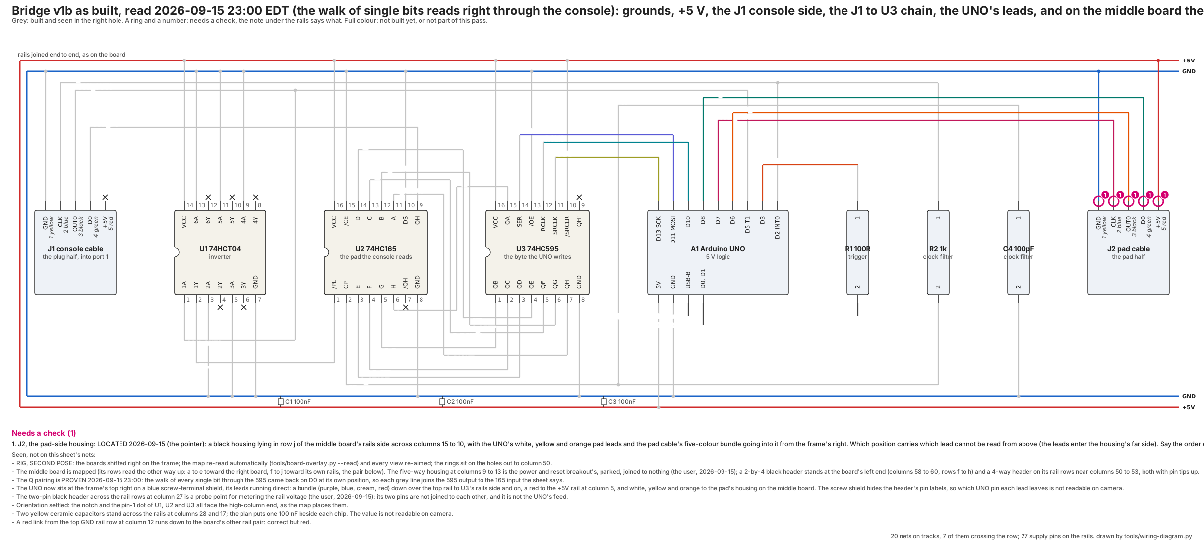
同じ図に、ビルドの状態を載せたもの。docs/build-status-v1b.json から (日付入りで、
ベンチを見た目で読んだもの): 灰色は組んで正しいと見えたところ、丸で囲んだ番号は
検査が要るところで、レールの下の注が何を検査するかを言い、はっきりした色はまだ
組んでいないところだ。状態ファイルを最後に読んだのは 2026-09-15 で、それ以来読み直して
いない。丸で囲んだ五つの検査は J2 のリードの順序で、それは 2026-09-18 にパッドが
ブリッジ越しに遊んで決着し、ヘッドの手 (2026-09-17) もその後に来た。
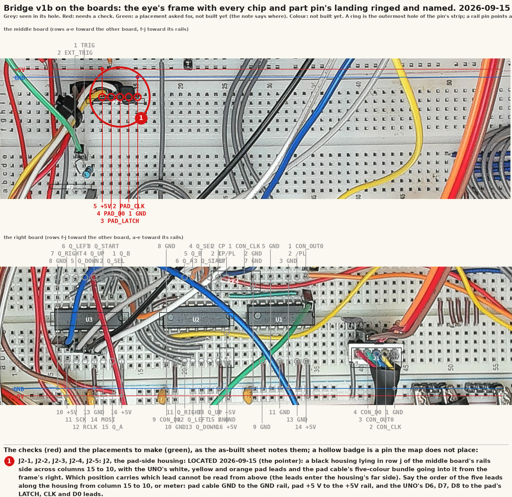
そして同じ状態を写真の上に。右のブレッドボードを目が捉えた枠、チップの全ピンの
着地点を丸で囲んで自分のネットの名を付け、灰色、桃色、はっきりした色はシートと
同じだ (tools/board-overlay.py。穴の格子は docs/board-map.json の中で一度だけ
枠から読み取ってあり、カメラの姿勢は一つ)。
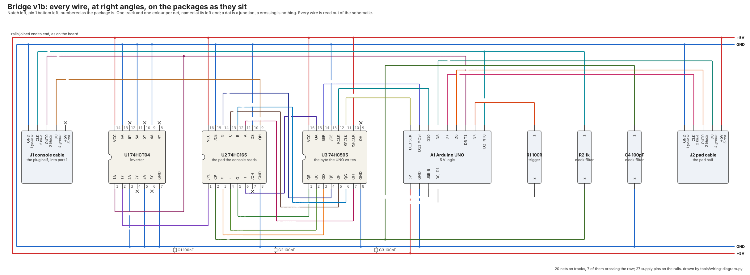
どのチップも自分のパッケージを上から見た姿で、切り欠きは左、1 番ピンは左下、
番号付けはパッケージのとおり。どの線も水平か垂直で、ネットごとに 1 本の道と 1 色、
名前は左端に、線が合流するところには点、ただ交差するだけのところには何も無い。
配線表と同じネットリストから tools/wiring-diagram.py が描くので、回路図に無い線を
見せることも、あるのに見せ落とすこともできず、道具は回路図が知らないピンを描くのを
拒む。2026-09-10 に、組むためのシートとしてブレッドボードの絵に取って代わった。
あの絵はいまも、各部品がどの穴に入るかを言う (breadboard-v1b.svg)。あちらの
曲がったジャンパを、こちらはまっすぐに直している。同じ日にインバータの空き入力
5 本が、注ではなく GND へ落としたピンとして回路図に載ったので、配線表はいま、
それを落とせと言う。
組む順序 (v1 のものを置き換える)
- ハーネスをメータで当たる (変更なし)。
- コンソールの電源を入れて、ポートをメータで当たる (変更なし)。
- もう一方のポートに差した純正のパッドを、四つのパルス幅についてスコープで見る (変更なし。これが書き下ろしの数字すべてを置き換える)。
- U1 + U2 に H..A の線を渡し、コンソールの電源を入れ、QH をスコープに: 模様が パッドの順で現れる。コンソール側だけを証明する。
- UNO + U3 + J2、コンソールの電源は切って:
STATUSが、ボタンに追従するパッドの バイトを見せる。SET 08は U3 の出力に 08 を置く (メータで当たる)。 - つなぐ: U3 の出力を U2 の入力へ、D5 と D2 を J1 の 3 番ピンと 2 番ピンへ、GND を
GND へ。コンソールの電源を入れ、
MODE PASS、ゲームを一本: L の行が、ラッチ あたり 8。 - トリガ、リセット、電源はこれまでどおり。
七つすべて完了: 1 から 6 は 2026-09-15 までに (milestone-2026-09-15-rig-and-bridge.md)、
7 は 2026-09-17 に。tools/bench-check.py がワークステーションから二度緑。
v1b が手放すもの
- C6 の 50 ns のグリッチフィルタと、二つ目のハードウェア計数器。UNO で空いている
外部タイマの入力は一つだけだ (T0 は
millisが使っている)。 - ブリッジの上の Wi-Fi と BLE。関係ない。ヘッドは Pi だ。
- v2 の、数える 6 本の線。あれは v2 を作るときに旧来の ESP32 (PCNT が 8 ユニット) に載り、UNO は 5 V のレジスタとパッドの側を持ち続ける。マイクロコントローラ二つが、 それぞれ自分の電圧領域にいて、つながるのは Pi の USB だけ。
v2b、v2 の UNO 版、2026-09-09 に追加
bench-v2b-1.svg から bench-v2b-4.svg は、横向きのレター 4 枚に載った一つの
回路図だ。v1b に、同じ SPI チェーンの上の 165/595 の対をもう一組と、5 V の出力が
そのまま UNO に入る LM1881 を足したもの。UNO の図面から最後の 74LVC245 を取り除き、
二つ目のマイクロコントローラも取り除く。数えるものはすべて UNO に着地し、Timer1 の
ハードウェアの入力は LATCH1 に、残りは割り込みだ。シートに付いてきた README は、
v1b、それから v2b を作れと言っている。
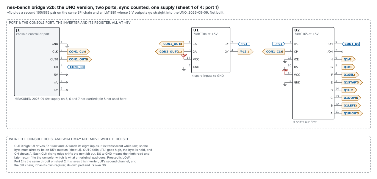
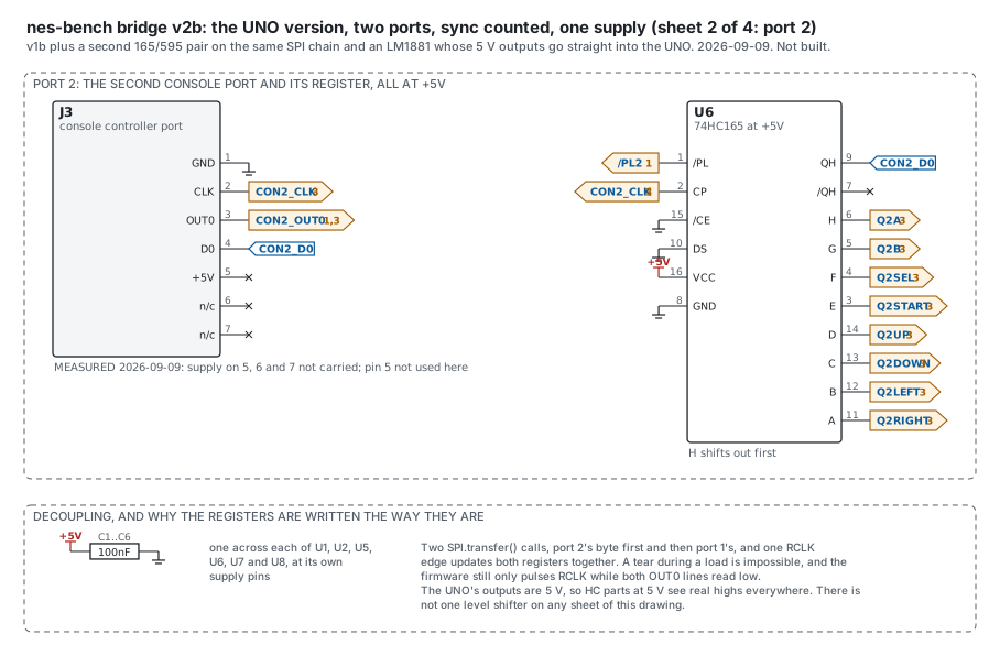
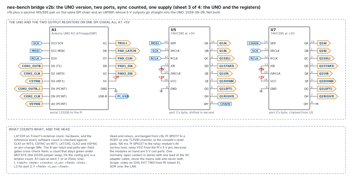
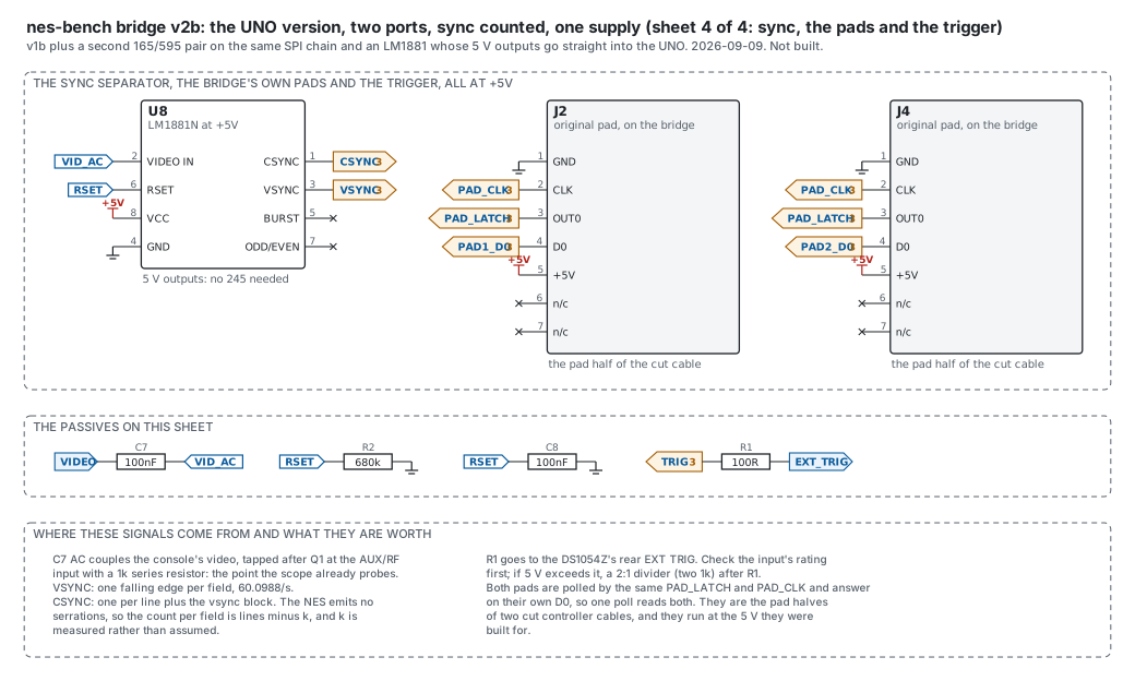
このシートのための基板は、配置と配線が済んでいる。2 層、裏面にグランドのベタ、
表面に電源、どのネットも通してあり、仕上がったファイルに未接続の項目もクリアランス
違反も無い。製造用の一式と、それを何に対して検査したかは
docs/fab/bench-v2b/README.md にある。
これについて二つのことが未決で、どちらも決まったものとして描くのではなく、ここで 名指ししておく:
- その L の行は 6 フィールドある、
L <latch> <byte> <clocks> <t_us> <field> <line>で、二番目のポートのためのL2と、フィールドごとのFの行も 付く。5 番目のフィールドがtools/b3.py、tools/compare-logs.py、head/headd.pyを壊すことは、この文書がすでに記録している。どれもちょうど 4 つを 要求する。だから v2b は、プロトコルの版と三つの道具を一緒に更新しなければ作れず、 それは見落としではなく、決めることだ。4 フィールドの行は v1b のもので、そのまま 残る。 - CSYNC の負荷は書き下ろしだ。 シートは、INT1 の 15.7 kHz は 16 MHz の部品の およそ 5 パーセントだと言う。あれは算術であって実測ではなく、しかも一つの UNO が 数える 6 本の線を全部背負えるかを決める数字だ。信じる前に測る。
ファームウェアを書いたときに入れた訂正、2026-09-08
スケッチは firmware/bridge-uno/bridge-uno.ino で、コンパイルできる。フラッシュ
8,018 バイト、24 パーセント、SRAM 1,521 バイト、74 パーセント。書いたことで、この
文書が未決にしていたか間違えていた六つのことが決まり、上の箇条はいま、計画したこと
ではなく作ったことを言っている。
SPI.transfer(b)はSPI.transfer(~b)にしなければならず、595 を通って 165 へ 入るビットの順は、仮定せずに筋を通して考えなければならなかった。どちらも黙って 鏡像になるバグだ。micros()のフィールドは、4 つを要求する三つの道具を壊していた。- MUTATE のジャンパとその D4 の設定ピンは要らない。ラッチの線の PCINT21 が、 ソフトウェアでそれをする。
- C6 の 2048 項目のスケジュールは入らなかったし、入りようも無かった。128 は実測で、 選んだ数ではなく、三箇所がいま、切り詰める代わりに拒む。(2026-09-19 に 600 へ 詰めた。「スケジュール、詰めた形」。2026-10-18 からはヘッドが流し込む輪。)
- 64 ビットの計数器は、この部品には存在しない。
- 手元にあるリレーモジュールは 5 V コイルのオプト入力の部品なので、v1 のシートの 3.3 V のレールはあれらにも間違っていた。両方のシートはいま、Pi の 5 V ピンと アクティブ低の入力を見せている。
それらすべての後で、部品が一つ変わった、2026-09-09: U1 はいま SN74HCT04N で、 HC04 ではない。 HCT の入力しきい値は HC の 3.5 V ではなく 2.0 V で、それが 2A03 の NMOS の OUT0 の出力で安全である理由だ。そして、この文書が抱えていた 「実測までは LS04」という保険も、それと一緒に消えた。同じ部品が C6 のシートの 3.3 V から 5 V への仕事を 2 ゲートでこなすので、一式のどこにも LS245 もプルアップも 残っていない。
コンパイラではなく計器から来た訂正が一つ。どちらのシートも、コンソールの映像を
スコープの CH1 に置いている。あれは CH3 だ。scope-capture.py がずっと既定にして
きたのはそこで、プローブが実際に座っているのもそこ (実測 2026-09-07、1,512 本の
同期パルス)。そして CH1 は B2 のマスタクロックのチャネルなので、図面は、位相合わせの
分類器が必要とする唯一のチャネルを、別の用途に使うと主張していた。
ビルド時に nes-bench/docs/bench-v1b-uno.md から取り込まれる。リポジトリが唯一の写しだ。報告書は独自の作業用語をいくつか使っている: 報告書で使われる言葉。