The v1b bridge on an Arduino UNO
Printable: NES controller-port bridge, v1b: drawing package TM-NESB-001 rev P (PDF); v1b as built, the checks called out on the photograph (PNG); NES controller-port bridge, v2b: drawing package TM-NESB-002 rev A (PDF); v2b board, top copper (SVG).
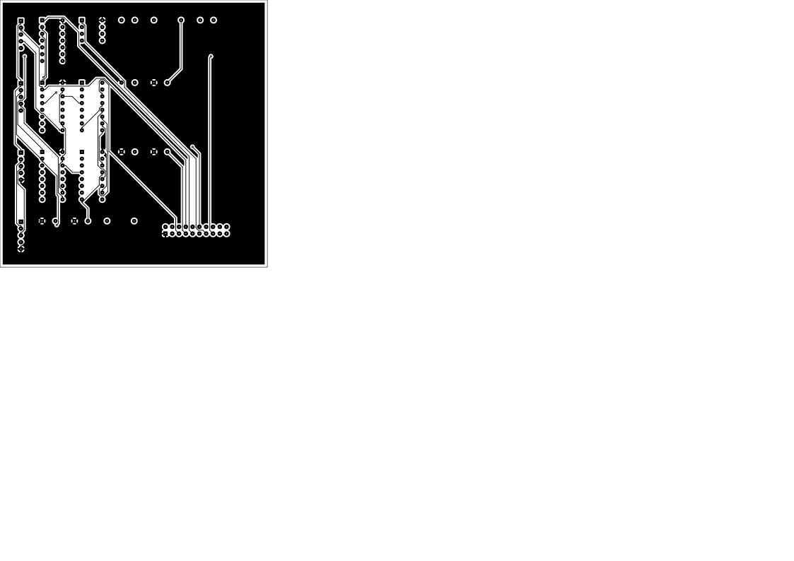
Added 2026-09-08 after the parts arrived. Supersedes v1 as the thing to build first; v1 stays in the set as the C6 version for when v2's counters need it.
Why
The 74HC parts that arrived (HC165, HC595) need a 3.5 V high at 5 V. The ESP32-C6 gives 3.3 V. The UNO's ATmega328P is a 5 V part, so with it in the middle every signal on the console side is 5 V and in spec, and three things fall out:
- No 74LVC245: the UNO reads the console's OUT0 and CLK directly.
- No 74LS245 up-shifter with pullups: the UNO drives the 595 at 5 V.
- The pad is polled at the 5 V it was built for. Measure-first item 4 (does the 4021 run at 3.3 V) no longer gates anything.
Parts (all on hand)
| ref | part | from |
|---|---|---|
| A1 | Arduino UNO R3 | the pile |
| U1 | SN74HCT04N | the tube that arrived 2026-09-09. HCT: 2.0 V input threshold, safe on the 2A03's NMOS OUT0 |
| U2 | SN74HC165N | the TI bag |
| U3 | SN74HC595N | the box of 30 |
| C1..C3 | 100 nF | |
| R2 | 1 k, CON_CLK to U2's CP | on hand; on the sheet since 2026-09-15 |
| C4 | 100 pF, CP to GND | on hand; on the sheet since 2026-09-15 |
| R1 | 100 R, the trigger into the scope's CH1 (the DS1054Z has no EXT TRIG; 2.5 V measured 2026-09-15) | |
| J1 | console port header harness | |
| J2 | the console's other port housing | |
| DIP-14 and DIP-16 sockets | the kit |
UNO pins
| pin | function | why this pin |
|---|---|---|
| D13, D11 | SCK, MOSI to U3 | hardware SPI, 4 MHz, 8 bits in 2 us |
| D10 | RCLK to U3 | one rising edge moves the byte; pulsed only while D5 reads low |
| D5 | CON_OUT0 | Timer1 external clock input (T1): a 16-bit hardware counter of latch rising edges. Also readable as a level for the write gate |
| D2 | CON_CLK | INT0, falling-edge ISR: clocks per poll |
| D3 | TRIG | rises at latch T, one loop late |
| D6, D7, D8 | PAD_LATCH, PAD_CLK, PAD_D0 | the bridge's own pad poll, at 5 V |
| D0, D1 | serial to the Pi over the UNO's USB | 115200 |
| 5V, GND | the bridge's supply and ground | from the Pi through USB |
Timer1 in external-clock mode counts edges synchronously with the 16 MHz clock, so a pulse must be longer than one CPU cycle (62.5 ns) to count; the console's latch pulse is microseconds. There is no glitch filter on this pin; if the L stream ever shows a latch count that is not one per poll, add a 100 pF to ground on D5 and record it. That is a different pin from the filter the sheet already carries: R2 and C4 sit on the 165's clock pin, against the spike measured on 2026-09-15.
Firmware, delta from bridge.ino
The protocol in docs/script.md is unchanged, so headd.py and the
tools need nothing beyond the serial speed.
write_register(b):SPI.transfer(~b), then ifdigitalRead(5)is LOW, pulse D10 high for one instruction and read D5 again; if it went HIGH across the pulse, flag the next L line. The complement is not cosmetic: pressed is LOW at the register. SPI is MSB first and the first bit sent travels furthest, so bit 7 sent first puts our bit 0 on QA, which is the A button. Reverse either and the pad is silently mirrored.- Latch count: read
TCNT1(16-bit), keep a 32-bit running total, handle wrap. Clock count: a volatile counter in the INT0 ISR. - Loop order: read counts, emit L, then write. Fixed 64-byte line
buffer, no
String. Schedule cursor, not a scan. - The schedule held 128 entries, not the C6's 2048. This part has
2 KB of SRAM in total and the compiler is the authority: at 256 it
reported 2161 bytes of globals, 105 percent, and refused to link; at
128 it reported 1521 and left 527 for the stack (the 2026-09-08
build; 1533 and 515 by 2026-09-18, the table below). Since 2026-09-19
it holds 600, packed (the section below, "How the bridge works"),
and since 2026-10-18 the 600 are a ring the head refills during the
run, so a record is no longer bounded by them (nes-bench 8f35ed6).
tools/fake-bridge.pymirrors the ring so a run can be rehearsed, and the head stops any run in which the bridge answers# schedule fullor# late. - There is no
Serial.printfon the AVR core and avr-libc's printf carries no 64-bit conversion, so the C6'suint64_tcounters and%lluwould have compiled to nothing useful. Every counter here isuint32_tand%lu: the latch index wraps after 2.2 years at 60 polls a second. - The L line stays at four fields,
L n hh c. A timestamp is v2'st_usand does not belong here:tools/b3.py,tools/compare-logs.pyandhead/headd.pyall require exactly four, so a fifth field would break the record, the comparison and the head's latch tracking at once. The head already timestamps what it receives. MUTATE ON: no jumper and no config pin. D5 is PD5, which is also PCINT21, so the latch line can raise a pin-change interrupt while Timer1 goes on counting it in hardware. Under MUTATE the clock counter is fed by that interrupt on rises only, and INT0 stops feeding it. That is B0's stated sabotage, the clock counter fed the latch line, done in software with nothing to forget to move back. A mutated run reports one clock per latch instead of eight, so the 8-per-latch gate is red.
How the bridge works: the UNO's job, its code and the ideas under it
This section is for a reader who wants to know what the Arduino is
actually doing between the console and the pad, line by line where it
matters. The sketch is firmware/bridge-uno/bridge-uno.ino with its
schedule in schedule.h; the head that drives it is head/headd.py.
The job in one paragraph
The console believes it is reading a controller. The UNO makes that
true with a controller of its own choosing. It sits in the cut cable
between the console's port and an original pad, and does four things
at once: it presents a byte to the console exactly where a pad's
buttons would be; it counts every time the console asks for the
buttons (a poll, or latch), which gives the bench a clock that the
part and the model share; it reads the original pad itself, so a hand
can play through it; and it reports all of that to the head over USB
serial, one line per poll. What it presents is either the hand's byte
(MODE PASS) or a byte from a schedule the head loaded (MODE INJECT). That is the whole trick behind replaying a person's play on
the console and on the model with the same inputs at the same polls.
How a console reads a pad
An NES pad is one 8-bit parallel-in, serial-out shift register (a 4021) and eight buttons. The console reads it in three moves, all from the game's own code:
- Strobe. The game writes 1 then 0 to
$4016; the console'sOUT0line goes high and low. While it is high the register copies the eight buttons in; the fall freezes them. That fall is the latch, and the bench counts time in latches: latch 0 is the first poll after the bridge'sRESET, and a Super Mario Bros. frame is one latch. - Shift. The game reads
$4016eight times. Each read pulses the console'sCLKline, and the register moves one bit onto the data line, in a fixed order: A, B, Select, Start, Up, Down, Left, Right. - Active low. A pressed button reads as 0 on the wire. The bench's byte is the other way up (bit 0 = A, set = pressed), and the firmware complements it on the way out.
The bridge's log line for each poll is L <latch> <byte> <clocks>:
the index, the byte the console was given, and how many clocks the
game spent reading it (eight for a normal poll, nine when a sample
fetch clocks the pad twice, which is a measured 2A03 behaviour).
The two chips that stand in for the pad
The console must see a shift register that behaves like the pad's, so
the bridge has one: a 74HC165, wired where the pad's 4021 was, loaded
by OUT0 and shifted by CLK, entirely by the console. The UNO never
touches its timing, which is the point: the console reads the bridge at
full speed with no software in the path.
The UNO sets the 165's eight parallel inputs through a second register,
a 74HC595, because the UNO does not have eight spare pins that change
together. The byte goes in serially over SPI (SPI.transfer), which
changes nothing yet, and one rising edge on RCLK (pin D10, the
PORTB |= _BV(PB2) line in write_register) moves all eight bits to
the 595's outputs at once. So the 165's inputs change in a single
62.5 ns step, never one bit at a time, and a poll can never read half
of an old byte and half of a new one from the shift.
Two details that were each a silent wrong answer if backwards: the
595's QA feeds the 165's H, and the 165 shifts H out first, so
QA is the A button; SPI sends the most significant bit first and the
first bit sent travels furthest, so sending bit 7 first leaves bit 0 on
QA. And the complement (reg_byte_for) is what makes a pressed
button a 0 on the wire. Reverse any one and the pad is mirrored.
The load window
The 165 copies its inputs for the whole time OUT0 is high. If
RCLK moved them inside that window, the console could latch a byte
in transition. write_register therefore reads the latch line before
the SPI transfer, after it, and after the RCLK edge: if the window is
open before the edge it defers the write to the next loop pass
(deferred), and if it opened across the edge it says so on the next
L line (torn). STATUS reports both counts; on the bench they have
stayed at zero.
Counting without missing: a hardware counter and a snapshot
At 60 polls a second a missed latch is a replay one frame out of step
for the rest of the run, so counting cannot depend on the loop being
quick. The latch line is on D5 because D5 is T1, Timer1's external
clock input: set up as a counter (TCCR1B = CS12|CS11|CS10), Timer1
counts the latch's rising edges in hardware whatever the processor is
doing. The console's clock line is on D2, INT0, and an interrupt
counts its falling edges.
The same D5 pin also raises a pin-change interrupt (PCINT21). Its
handler asks Timer1 whether the count moved (a rise, not a fall, is
told apart by the counter rather than by reading the pin, because the
latch pulse is 3.6 microseconds wide and the interrupt can arrive after
it has ended), and if so it records, in the same instant, the clock
count at that rise (clocks_at_rise) and the number of rises. The
loop later reads that pair with interrupts off. Both rules were
measured into existence on 2026-09-15: reading the pin missed 7 of
1,202 latches, and reading the two counters a few instructions apart
booked clocks to the wrong poll.
The loop
loop() runs about every 100 microseconds, in a fixed order:
- Commands. Bytes from the serial port are gathered into a 64-byte
line buffer and each complete line is handled (
handle). - The pad. Once a millisecond the UNO polls the original pad on
its own three pins (
poll_pad, the same strobe-and-shift the console does, at leisure), keeping the result aspad_byte. - Book the polls. If the interrupt has seen new latch rises, the
loop prints the
Lline for the poll that just ended, with the byte the register held for it and the clocks between its rise and the one before; then it advances the latch index. Printing before writing a new byte is what makes theLline's byte the one the console actually read. - The trigger. If
TRIG nis armed and latch n has passed, D3 goes high for a millisecond: the scope's trigger, on CH1. - The byte. In
PASSthe wanted byte is the pad's; inINJECTit is the schedule's for the current latch. If it differs from what the register holds,write_registerchanges it.
The line protocol
The head talks to the bridge in short text lines at 115200 baud, and
the bridge answers each with a # line: MODE PASS|INJECT, SET hh
(the byte to hold now), AT n hh (from latch n on, hold hh; n must
not go backwards), TRIG n, RESET (zero the counters, clear the
schedule and the trigger), STATUS, and MUTATE ON|OFF (B0's
sabotage: the clock counter fed from the latch line, so the
eight-clocks check must fail). A line it cannot parse comes back as
# ? ....
The head waits for each line's answer before it sends the next, and
checks that an AT's answer carries the latch and byte it sent. It did
not always: on 2026-09-18 a hand's record of 125 AT lines, sent back
to back, overran the UNO's 64-byte receive buffer, some lines came back
# ?, others were taken with digits missing (AT 2219 00 as at 2210 00), and Mario ran the wrong way on the replay while every check stayed
quiet. The head also drops its count of latches when it sees the
bridge's # reset, so a WAIT n after a reset cannot be satisfied by
the session before (the cold-boot "Start is ignored" finding of the same
day was exactly that).
Waiting for every echo made loading slow: a whole minute's schedule,
290 lines (289 changes of the byte and the opening SET), takes about
15 seconds. So the head holds the console in reset from RESET through
the SET, AT, TRIG and ARM lines that
follow and lets it go at the first other word (after half a second at
least), and latch 0 is still the release. Before that, the replay's
TRIG 1000 arrived at latch 1060, the bridge fired it at the next latch
as it was built to, and two captures of the game 60 frames on read as a
divergence. A TRIG whose latch has already passed now stops the run.
The schedule, packed
AT n hh means: from latch n on, hold hh, until the next entry. The
protocol keeps n absolute, and so do the head, the tools and the C6
build. Only the UNO's RAM holds it differently, because it has 2048
bytes in total and the first build spent five of them per entry (a
32-bit latch and a byte), which held 128 entries. A minute of a hand
playing Super Mario Bros. through 1-1 is 289 changes of the byte.
schedule.h stores each entry as two bytes: the GAP in latches from
the previous entry (0 to 254), and the byte. A gap of 255 or more is
paid for with FILLER entries, each "advance 255 latches, change
nothing" (the gap value 255 is reserved for them), so a filler never
has to name a byte. append converts an absolute n into fillers and an
entry, refusing whole if they do not fit (# schedule full) and
refusing an n before the last one. due walks a cursor forward as the
latch index grows, adding up the gaps, and applies every entry whose
latch has come; it copes with the index jumping by more than one,
which happens when the loop was busy.
Since 2026-10-18 the 600 slots are a ring. An applied entry frees its
slot, so the head can append behind the cursor while the console
plays: it loads 480 entries before the console leaves reset and feeds
the rest as the L lines show the latches going by, a few dozen at a
time. An AT for a latch that has already fallen is refused
(# late AT n at latch L) rather than applied a poll late, and the
head fails the run on it, as it does on # schedule full and on a run
that ends with lines still unsent. A streamed run takes no scope
CAPTURE partway, because the head is busy feeding the bridge. It was
proven on the part with Super Mario Bros.: one schedule of 618 entries
from power-on through 3-4 (run 20261018-145621), every one of its
27,683 polls in the log and none wrong.
What paid for the room:
| build | entry | entries | globals | left for the stack |
|---|---|---|---|---|
| to 2026-09-18 | 5 bytes | 128 | 1533 bytes | 515 |
| packed | 2 bytes | 320 | 1615 | 433 |
| packed, strings in flash | 2 bytes | 320 | 967 | 1081 |
| packed, strings in flash (flashed) | 2 bytes | 600 | 1527 | 521 |
The second row is the surprise worth knowing about the AVR: a plain
string literal is copied from flash into RAM at boot, so every message
the sketch prints cost RAM, and two new messages cost 82 bytes. Every
literal now stays in flash (F("..."), PSTR, snprintf_P,
strcmp_P; a flash string passed to % needs %S), which gave back
648 bytes. The schedule then grew until the stack had what the old
build ran on.
The compiler's figure is an estimate of the stack; the firmware
measures it. setup paints the free RAM between the globals and the
stack with 0x5A, and STATUS counts how much paint is still intact
(# stack N bytes never touched). After a full minute's schedule was
loaded and replayed it read 355 bytes never touched: the stack's
deepest reach was about 130 bytes.
The packing is tested off the chip. tools/test-uno-schedule.sh
builds schedule.h natively and plays 400 random schedules (gaps from
0 to 2000, entries past latch 254 so fillers come first, latch indices
that jump) and any real record against the protocol's absolute
meaning, latch by latch, plus the capacity edge; MUTATE=1 makes a
filler set the byte to zero and must fail (it fails 384 of 402). The
same schedules are also streamed through a 64-slot ring, fed as the
latches go by (601 cases in all); MUTATE_RING=1 makes the cursor
wrap a slot short and must fail. tools/b3.py record counts a record
in packed entries by the same rule (entries_for) and names a record
longer than the ring, which the head will stream, instead of refusing
it; tools/fake-bridge.py keeps the same ring and refuses what the
UNO refuses.
What the bridge still cannot do
It holds 600 entries at a time, and longer runs are streamed, so the schedule's length is bounded by the run, not the RAM; what is still bounded is how far ahead the head can be, 600 entries. It does not watch the console's data line (D0 is not wired back), so what the console actually shifted out is inferred from the register and the clock count, not read. And it serves one port: the second controller is not bridged.
The wiring, drawn to build from
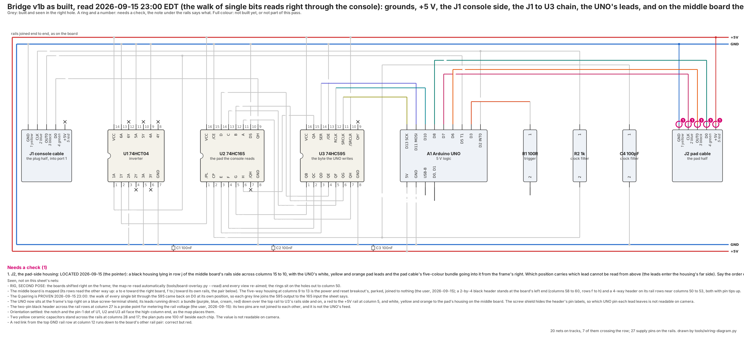
The same drawing with the build's state on it, from docs/build-status-v1b.json
(dated, read off the bench's eye): grey is built and seen right, a ringed number
needs a check and the note under the rails says what, full colour is not built yet.
The state file was last read on 2026-09-15 and has not been re-read since: the five
ringed checks are J2's lead order, which the pad playing through the bridge settled
on 2026-09-18, and the head's hands (2026-09-17) came after it.
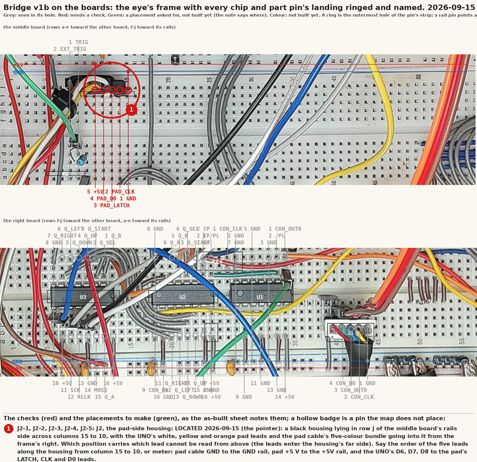
And the same state on the photograph: the eye's frame of the right
breadboard, every chip pin's landing ringed and named with its net,
grey, pink and colour as on the sheet (tools/board-overlay.py, the
hole grid read off the frame once in docs/board-map.json, one camera
pose).
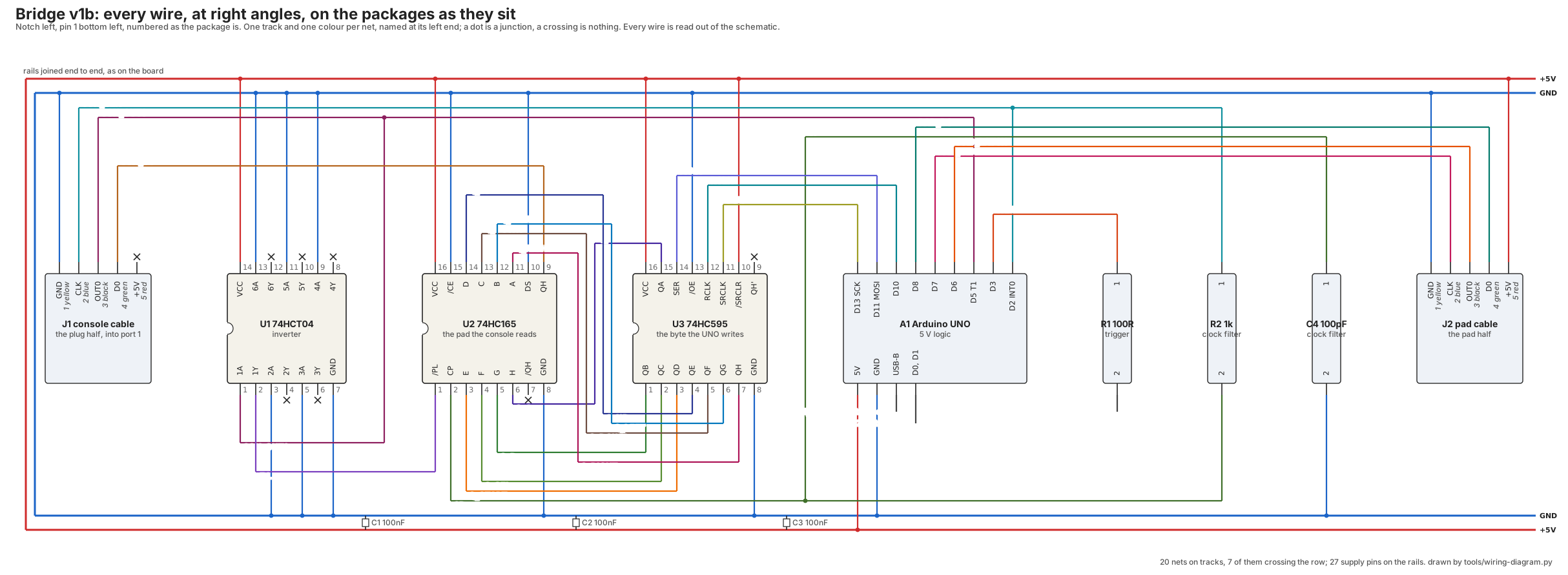
Each chip is its package seen from above, notch left, pin 1 bottom
left, numbered as the package is; every wire is horizontal or vertical,
one track and one colour per net, named at its left end, a dot where
wires join and nothing where they merely cross. Drawn by
tools/wiring-diagram.py from the same netlist as the wiring list, so
it cannot show a wire the schematic lacks or lack one it has, and the
tool refuses to draw a pin the schematic does not know. It replaced the
breadboard picture as the sheet to build from on 2026-09-10: that
picture still says which hole each part goes in (breadboard-v1b.svg),
and its curved jumpers are what this one straightens out. The same
day the inverter's five spare inputs went onto the schematic as pins
tied to GND rather than a note, so the wiring list now says to tie them.
Build order (replaces v1's)
- Meter the harness (unchanged).
- Meter the port with the console on (unchanged).
- Scope the original pad in the other port for the four pulse widths (unchanged; these replace every authored number).
- U1 + U2 + wire links on H..A, console on, QH on the scope: the pattern appears in pad order. Proves the console side alone.
- UNO + U3 + J2, console off:
STATUSshows the pad byte following the buttons;SET 08puts 08 on U3's outputs (meter them). - Join: U3 outputs to U2 inputs, D5 and D2 to J1 pins 3 and 2, GND
to GND. Console on,
MODE PASS, a game: L lines, 8 per latch. - Trigger, reset, power as before.
All seven done: 1 to 6 by 2026-09-15 (milestone-2026-09-15-rig-and-bridge.md),
7 on 2026-09-17, tools/bench-check.py green twice from the workstation.
What v1b gives up
- The C6's 50 ns glitch filter and its second hardware counter. The
UNO has one external timer input free (T0 is used by
millis). - Wi-Fi and BLE on the bridge. Irrelevant; the Pi is the head.
- v2's six counted lines. Those go on the classic ESP32 (8 PCNT units) when v2 is built, with the UNO still owning the 5 V register and pad side. Two microcontrollers, each in its own voltage domain, joined only by the Pi's USB.
v2b, the UNO version of v2, added 2026-09-09
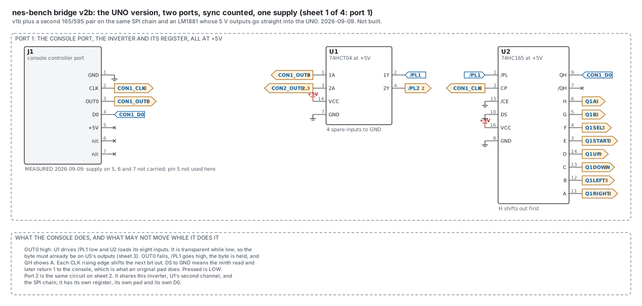
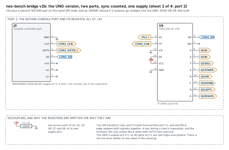
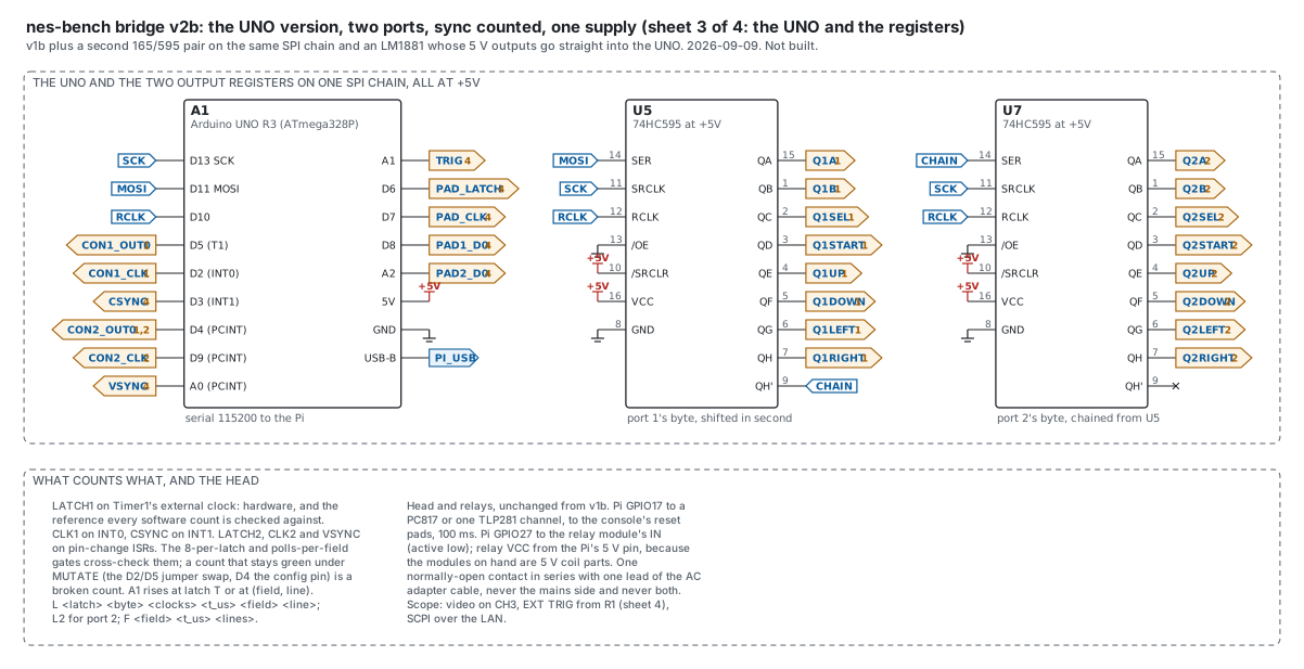
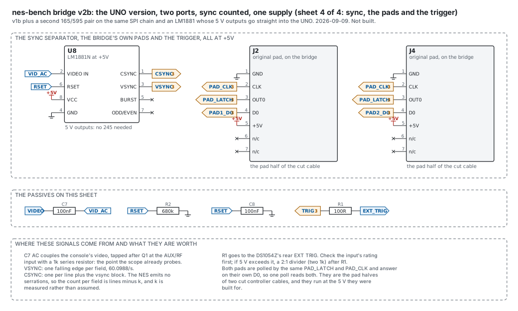
bench-v2b-1.svg to bench-v2b-4.svg are one schematic on four
landscape letter sheets: v1b plus a second 165/595 pair on the same SPI
chain and an LM1881 whose 5 V outputs go straight into the UNO. It
removes the last 74LVC245 from the UNO designs and it removes the second
microcontroller: every count lands on the UNO, Timer1's hardware input
on LATCH1 and interrupts for the rest. The README that came with the
sheets says to build v1b, then v2b.
The board for these sheets is placed and routed: two layers, ground
poured on the back and supply on the front, every net carried, and no
unconnected item or clearance violation on the finished file. The
fabrication set and what it was checked against are in
docs/fab/bench-v2b/README.md.
Two things about it are open, and both are named here rather than drawn as settled:
- Its L line has six fields,
L <latch> <byte> <clocks> <t_us> <field> <line>, plusL2for the second port and anFline per field. This document already records that a fifth field breakstools/b3.py,tools/compare-logs.pyandhead/headd.py, all of which require exactly four. v2b therefore cannot be built without a protocol version and three tools updated together, and that is a decision, not an oversight. The four field line is v1b's and stays. - The CSYNC load is authored. The sheet says 15.7 kHz on INT1 is about 5 percent of a 16 MHz part. That is arithmetic, not a measurement, and it is the number that decides whether one UNO can carry all six counted lines. Measure it before trusting it.
Amendments made when the firmware was written, 2026-09-08
The sketch is firmware/bridge-uno/bridge-uno.ino, and it compiles:
8,018 bytes of flash, 24 percent, and 1,521 bytes of SRAM, 74 percent.
Writing it settled six things this document had left open or wrong, and
the bullets above now say what was built rather than what was planned.
SPI.transfer(b)had to becomeSPI.transfer(~b), and the bit order through the 595 into the 165 had to be reasoned about rather than assumed. Both are silent-mirror bugs.- The
micros()field would have broken three tools that require four. - The MUTATE jumper and its D4 config pin are not needed; PCINT21 on the latch line does it in software.
- The C6's 2048-entry schedule did not fit and never could; 128 was measured, not chosen, and three places now refuse rather than truncate. (Packed to 600 on 2026-09-19: "The schedule, packed"; a ring streamed by the head since 2026-10-18.)
- The 64-bit counters do not exist on this part.
- The relay modules on hand are 5 V coil parts with opto inputs, so the v1 sheet's 3.3 V rail was wrong for them too; both sheets now show the Pi's 5 V pin and an active-low input.
One part changed after all of that, 2026-09-09: U1 is an SN74HCT04N now, not an HC04. HCT's input threshold is 2.0 V rather than HC's 3.5 V, which is what makes it safe on the 2A03's NMOS OUT0 output, and the "LS04 until measured" hedge this document carried is gone with it. The same part does the C6 sheets' 3.3 V to 5 V job in two gates, so no LS245 and no pullups remain anywhere in the set.
One correction that came from the instrument rather than the compiler:
both sheets put the console's video on the scope's CH1. It is on CH3.
That is where scope-capture.py has always defaulted, it is where the
probe actually sits (measured 2026-09-07, 1,512 sync pulses), and CH1
is B2's master-clock channel, so the drawing was claiming the one
channel the alignment classifier needs for something else.
Pulled at build time from nes-bench/docs/bench-v1b-uno.md; the repository is the one copy. The reports use some working words of their own: Words the reports use.