What is in the pile
Gear on hand for new projects, read off the owner's photographs. Each entry says what was READ off the part (silkscreen, chip marking, resistor code) and what comes from the part family's documentation, which is not a measurement. Nothing here has been powered on this bench unless it says so.
The cartridge pile (the 65C02 set, the static RAM, the mask ROM
adapter) is in cal-cart-build.md; the bridge's own parts are in
parts.md.
Photographed 2026-10-05: three ESP32 boards and two opto boards
| item | marking read | what it is | fits |
|---|---|---|---|
| Stamp P4 | STAMP P4; ESP32-P4NRW32; XMC 25QH128 | ESP32-P4 core board, no radio, no buttons, castellated | pad-usb (it runs it now); camera/display work |
| C6 DevKitC | ESP32-C6-DevKitC-1 V1.2; ESP32-C6-WROOM-1 MCN8 | Espressif's C6 devkit, two USB-C | nothing: dead, set aside |
| C6 LCD | ESP32-C6-LCD-1.47 (Waveshare) | C6 board with a 1.47 in LCD and a card slot | the TRNG emitter (geiger TM-TRNG-001) |
| HW-399 | Optoisolator HW-399; TLP281-4 GB | four isolated channels, slow | isolating buttons, relays, slow logic |
| Iso_817_X1 | Iso_817_X1_V1.1; P785 GB | one isolated channel, terminals | the TRNG case's stand-in opto |
Stamp P4: the board that boots straight into the pad firmware
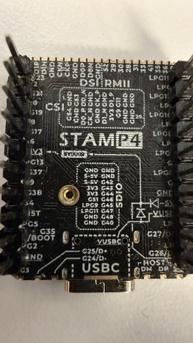
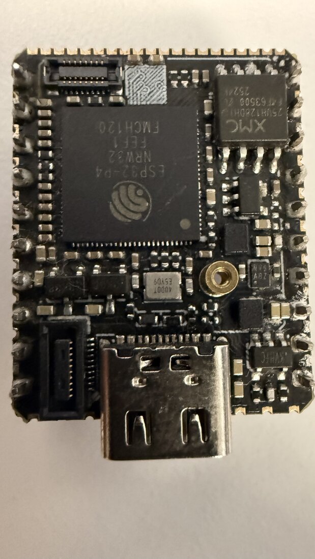
- Read: ESP32-P4NRW32 (the P4 with 32 MB of PSRAM in the package), flash XMC 25QH128 (128 Mbit, 16 MB), STAMP P4 on the silkscreen. The maker's name is not printed on the board.
- Silkscreen groups: CSI (camera, FPC connector on the part side), DSI (display), RMII (Ethernet MAC pins), SDIO, LPG (low-power GPIO), 5V, 3V3, RST, and G35/BOOT on the left edge.
- USB: one Type-C, wired to G24/G25 (D-/D+), the full-speed port that is normally the P4's USB serial/JTAG. HOST DM/DP pads at the bottom edge are the high-speed port.
- No buttons. To reach the ROM bootloader, hold G35/BOOT to GND while RST is pulled low and released (or while it powers up).
- This is very likely LITTLEGUY (the office machine, 2026-10-05): a P4, no
buttons, enumerating as
303a:0002 tinymachines NES Pad.firmware/pad-usbswaps exactly this port (PHY 0, GPIO24/25) to the OTG controller, which is why the board shows no serial port: its only socket is the pad. Unconfirmed until the bootloader answers. - From the family's documentation, not measured: no Wi-Fi or BLE on any P4; dual RISC-V high-performance cores plus a low-power core.
C6 DevKitC: the board that died, set aside
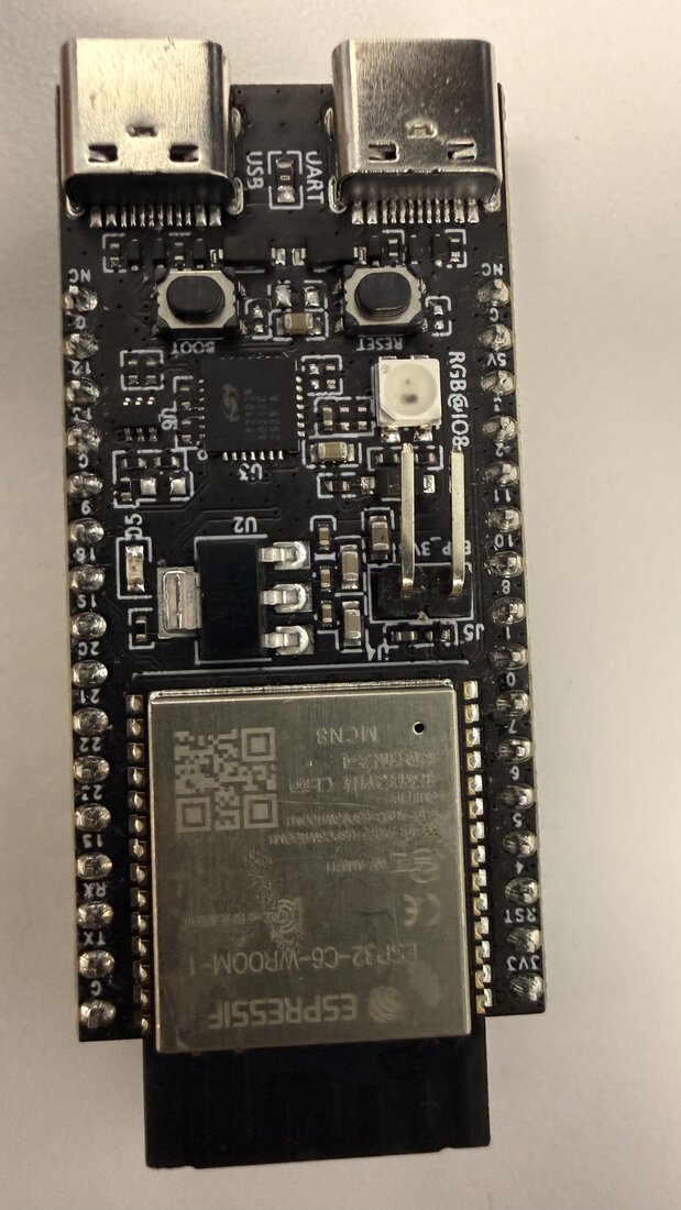
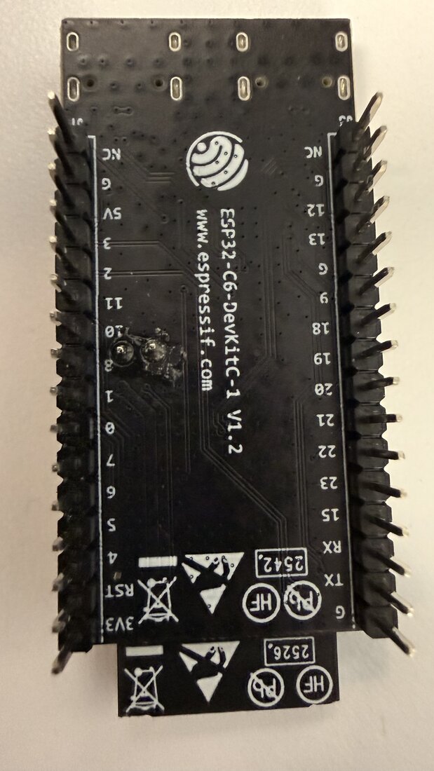
- Read: ESP32-C6-DevKitC-1 V1.2, module ESP32-C6-WROOM-1 marked MCN8 (8 MB flash), date codes 2542 and 2526 on the back. Two Type-C sockets marked USB (the C6's own USB serial/JTAG) and UART (through the bridge chip U3). BOOT and RESET buttons, RGB LED on IO8, jumper J5.
- Dead, and set aside (owner, 2026-10-05). This is the C6 devkit the pad sheets were drawn around, found dead on 2026-09-29 (no ROM banner on either socket); the flux and solder at the header pins labelled 10 and 8 on the back are from that build. Nothing is planned on it.
- From the family's documentation: Wi-Fi 6 (2.4 GHz), BLE 5, 802.15.4 (Thread, Zigbee), one RISC-V core.
C6 LCD: a C6 with a screen and a card slot
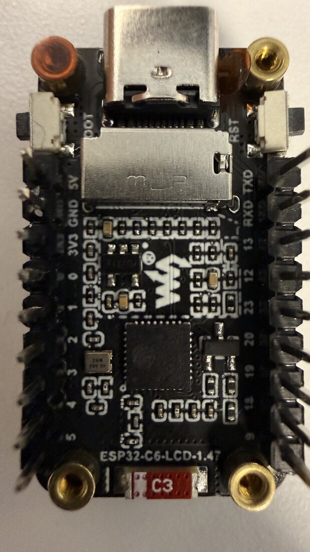
- Read: ESP32-C6-LCD-1.47, Waveshare logo, a 40.000 MHz crystal, one Type-C, BOOT and RST buttons, a card slot under the metal cage, header pins 0 to 5, 9, 18, 19, 20, 23, 12, 13, RXD, TXD, 3V3, GND, 5V. A red label reads C3 (someone's tag; the chip is a C6).
- The screen is on the other face; the photograph of it is out of focus and is not kept. Its size is in the product name, 1.47 in.
- Measured 2026-10-05 (
esp-reset --characterizeon the bench head): ESP32-C6FH8 (QFN32) rev v0.2, 8 MB flash in the package, 40 MHz crystal, base MAC b0:a6:04:8b:48:58, secure boot and flash encryption off, every key block empty. It enumerates as303a:1001, the C6's own USB serial/JTAG. - What it was running:
firmware/pad-ble(it printed "advertising as NES Pad"), which never lights the screen: that is the dark screen, not a fault. - From the vendor's wiki (waveshare.com/wiki/ESP32-C6-LCD-1.47, read 2026-10-05): ST7789 panel, 172 by 320; LCD on GPIO6 (MOSI), 7 (SCLK), 14 (CS), 15 (DC), 21 (RST), 22 (backlight); the card slot on 4 (CS) and 5 (MISO) sharing 6 and 7; the RGB LED on GPIO8. The wiki says 4 MB of flash; the chip says 8.
- Its job: the TRNG emitter, capture on GPIO18 (geiger
docs/HARDEN-PLAN.md).
HW-399: four channels, for slow signals
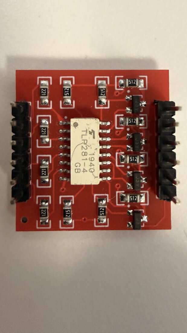
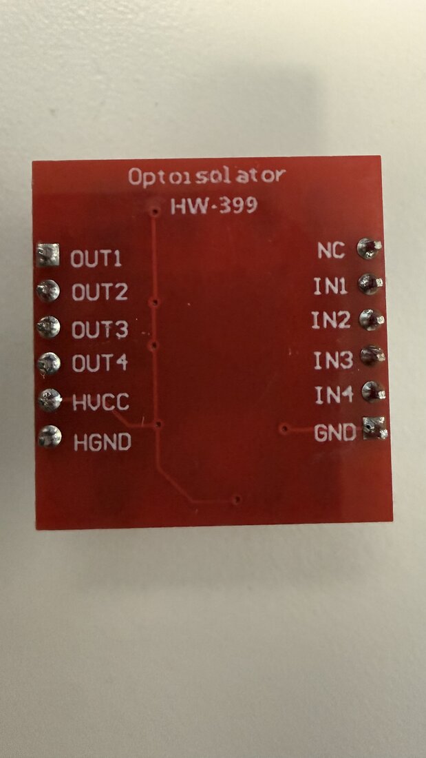
- Read: Optoisolator HW-399, Toshiba TLP281-4 GB (four phototransistor optocouplers in one package, date 1940), resistors coded 221 (220 ohm, one per input) and 512 (5.1 k), and four SOT-23 transistors marked J3Y. Pins: IN1 to IN4, GND, NC on the input side; OUT1 to OUT4, HVCC, HGND on the isolated side.
- Not measured: the output polarity (whether OUTn goes high or low when INn is driven) and its edge times. A phototransistor part like this one switches in microseconds; it is for buttons, relays and slow logic, not for timestamps.
Iso_817_X1: one channel, screw terminals
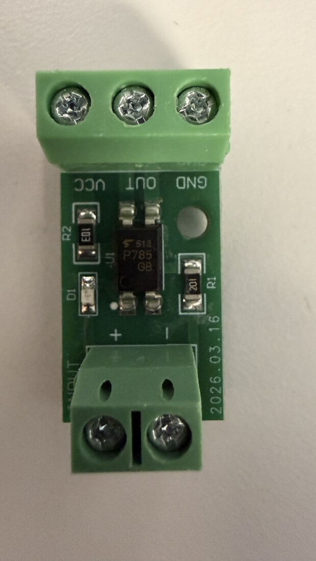
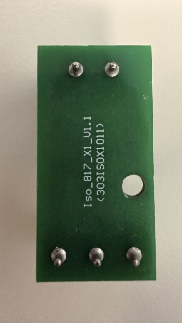
- Read: Iso_817_X1_V1.1 (303ISOX1011) on the back, 2026.03.16 on the front, and a Toshiba TLP785 GB on it, not a PC817 (the TLP785 is the same four-pin phototransistor class). Input terminals + and -, output terminals VCC, OUT, GND; indicator D1.
- The resistors, read with the board's own text turned upright: R1 = 102, 1 k on the input side and R2 = 103, 10 k on the output side. The markings are printed at right angles to the terminals' labels, and read the other way they would say 201 and E01; a meter settles it in seconds.
- The same model is the NES head's reset opto (
wiring.md,Iso_817_X1), so this R1 is the best reading so far of that one's input resistor too, and of the TRNG drawing's stand-in (geiger TM-TRNG-001 sheet 3 assumed 1 k).
Photographed 2026-10-06: an HP-16C
| item | marking read | what it is | fits |
|---|---|---|---|
| HP-16C | hp 16C; HEWLETT-PACKARD; USA, 2447A on the case | HP's programmer's calculator, the Voyager case | an independent oracle for the 6502's integer arithmetic |
HP-16C: the 6502's arithmetic in a pocket
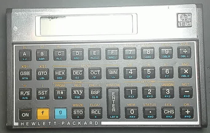
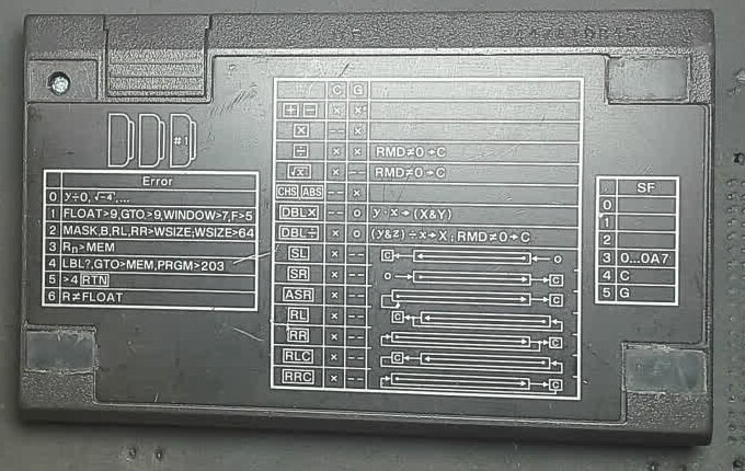
- Read off the bench camera: the 16C badge, the keyboard (HEX, DEC, OCT, BIN; SL, SR, RL, RR, RLC, RRC, ASR; MASKL, MASKR; AND, OR, XOR, NOT; WSIZE; 1's, 2's and UNSGN under SET COMPL), and the reference card moulded on the back: error codes 0 to 6, which operations set carry (C) and out-of-range (G), the shift and rotate diagrams, and flags 0 to 5.
- The serial is moulded along the top edge: USA, and a prefix that reads 2447A. By HP's convention that is 1984, week 47, made in the USA; the remaining digits are too faint for the overhead camera.
- The display was blank in the frame: off, or its three button cells (LR44 or SR44) are flat. Not yet powered on this bench.
- From the family's documentation: integer word sizes from 1 to 64 bits, signed in 1's or 2's complement or unsigned, with carry and out-of-range flags; HP's Nut processor inside.
- Why it is here: at word size 8 in 2's complement it computes what the 6502 computes (ADC carry and overflow, ASL, LSR, ROL, ROR), and it shares nothing with the simulator. The same kind of witness the published instruction table is for timing.
Pulled at build time from nes-bench/docs/pile.md; the repository is the one copy. The reports use some working words of their own: Words the reports use.