The bench cheat sheet
Printable: NES controller-port bridge, v1b: drawing package TM-NESB-001 rev P (PDF); v1b as built, the checks called out on the photograph (PNG).
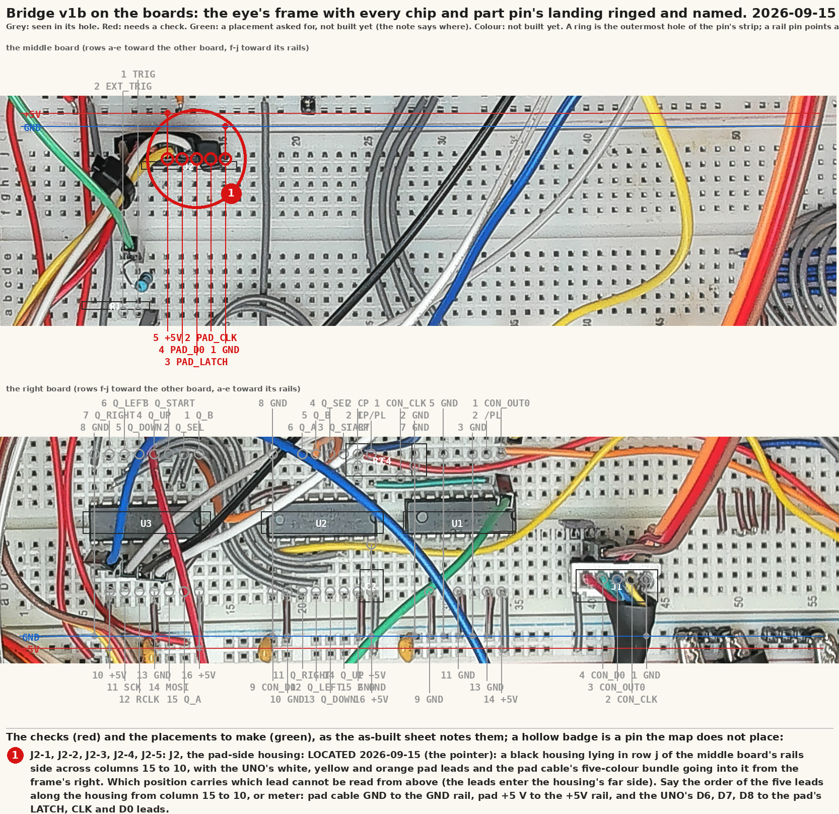
Generated by tools/cheatsheet.py. The pin numbers and signals are read out of
the schematic, the harness colours out of the lab log, the breakout leads out of
the bring-up tool's own table, and each chip's wiring out of the netlist. The only
authored text is what each pin does on the part, which is the datasheet's, kept
in one place in that tool and refused if the schematic names a pin differently.
The same rows are sheets of the drawing package (tools/make-package.py).
The head's hands (the Pi's jumpers, the PC817 and the relay) have their own:
cheat-sheet-head.md.
Sheet: bench-v1b.
The controller port: pin, NES harness, breakout
Pin numbers are the ones moulded into this console's port housing and the signals are the schematic's, MEASURED 2026-09-09 (the supply is on 5, not 7). Harness colours from the lab log, step 1.1 (2026-09-08). Breakout leads rung out 2026-09-09 with the cable out of the console; the pad half of the cut carries the same five colours. Use the lead, not the colour rule.
| pin | signal | NES harness | breakout lead | on the bridge |
|---|---|---|---|---|
| 1 | GND | brown | yellow | the GND rail |
| 2 | CLK | red | blue | R2-1, A1 D2 (INT0) |
| 3 | OUT0 | orange | black | U1-1, A1 D5 (T1) |
| 4 | D0 | yellow | green | U2-9 |
| 5 | +5V | white | red | not used: the bridge runs from the UNO's 5 V |
| 6 | n/c | blue | not carried | |
| 7 | n/c | purple | not carried |
The power and reset breakout
Five ways straight through, colour for colour with the front panel's harness (docs/lab/06-breakout-map-power-reset.jpg), metered 2026-09-17. No way is ground: the front panel is grounded by its pad and housing.
| pin | NES harness | breakout lead | what it is |
|---|---|---|---|
| 1 | brown | brown | power switch |
| 2 | red | red | power switch |
| 3 | orange | orange | reset, + side (4.40 V) |
| 4 | yellow | yellow | reset, - side, and LED |
| 5 | white | white | LED |
The head's four jumpers
Four Dupont leads off the Pi's header, no breakout (2026-09-10). Header positions are the Pi's own numbering. No wire from here to the console: the Pi's ground reaches it through the UNO's USB cable only.
| Pi pin | pos. | to | role |
|---|---|---|---|
| GPIO17 | 11 | PC817 module INPUT + | reset, 100 ms high |
| GPIO27 | 13 | relay module IN | power: high is on |
| 5V | 2 | relay module VCC | the coil's supply |
| GND | 6 | PC817 IN-, relay GND | the one ground lent |
The UNO ribbon
Nine Dupont wires from the UNO's digital header, colour per pin as read off the header (2026-09-11). The net and the far end come from the schematic.
| UNO pin | colour | net | to |
|---|---|---|---|
| D2 | blue | CON_CLK | J1-2, R2-1 |
| D3 | green | TRIG | R1-1 |
| D5 | yellow | CON_OUT0 | J1-3, U1-1 |
| D6 | orange | PAD_LATCH | J2-3 |
| D7 | red | PAD_CLK | J2-2 |
| D8 | brown | PAD_D0 | J2-4 |
| D10 | black | RCLK | U3-12 |
| D11 | white | MOSI | U3-14 |
| D13 | grey | SCK | U3-11 |
The scope: channels and the trigger
As wired 2026-09-15, each probe's landing given as a board column so it can be put back. Probe grounds on the right board's GND rail, which is the console's ground; probes on 10x. The DS1054Z has no external trigger input (MEASURED 2026-09-15), so the bridge's TRIG takes CH1, the channel held for the master clock until the mainboard is probed. Step 6.1 of the bring-up arms the scope on CH1 and fires TRIG at a latch.
| input | signal | probe on | why |
|---|---|---|---|
| CH1 | TRIG | R1 on the middle board: the resistor in row a from column 9 (the green D3 lead's housing) to column 6 (the red lead to the scope) | the trigger: 2.5 V rising at latch T, 5.4 V for 874 us (MEASURED 2026-09-15); the master clock's channel later, by turns |
| CH2 | CON_OUT0 (latch) | U1 pin 1: right board column 34, the side toward U2 (rows f to j) | one pulse per poll, 3.6 us wide, 60.06 a second; a new lead 2026-09-15 evening |
| CH3 | composite video | the console's video out, through the splitter | the picture the poll lands in |
| CH4 | CON_D0 | U2 pin 9: right board column 18, the rails side (rows a to e) | the byte the console reads back, pressed LOW: high through the eight bits for 00, low for ff (MEASURED 2026-09-15 23:00, which is how the two probes were told apart) |
| EXT TRIG | none | not on this scope | the DS1054Z has no external trigger input (MEASURED 2026-09-15: source EXT refused; the rear BNC is Trig Out) |
U1: 74HCT04 at +5V
Hex inverter, six independent gates. HCT inputs switch at TTL levels (high from 2.0 V), which is why it sits on the console's NMOS OUT0 line: OUT0 high loads the register, so its inversion is the 165's active-low load. One gate is used. The other five inputs are CMOS and must not float: tie each spare A input to GND and leave its Y open.
| pin | name | on the part | on this bench |
|---|---|---|---|
| 1 | 1A | gate 1 input | CON_OUT0: J1-3, A1 D5 (T1) |
| 2 | 1Y | gate 1 output, the inverse of 1A | /PL: U2-1 |
| 3 | 2A | gate 2 input | the GND rail |
| 4 | 2Y | gate 2 output | no connection |
| 5 | 3A | gate 3 input | the GND rail |
| 6 | 3Y | gate 3 output | no connection |
| 7 | GND | ground | the GND rail |
| 8 | 4Y | gate 4 output | no connection |
| 9 | 4A | gate 4 input | the GND rail |
| 10 | 5Y | gate 5 output | no connection |
| 11 | 5A | gate 5 input | the GND rail |
| 12 | 6Y | gate 6 output | no connection |
| 13 | 6A | gate 6 input | the GND rail |
| 14 | VCC | supply, 4.5 to 5.5 V; 100 nF to GND at the pin | the +5V rail |
U2: 74HC165 at +5V (the TI bag)
8-bit parallel-in, serial-out shift register: the pad's 4021 in a 74 package. While /PL is low the eight inputs A to H are copied into the stages as they are (it is transparent, so the byte must be settled before the load). With /PL high, each rising edge of CP shifts one place toward QH and pulls DS in at A. QH shows stage H, so H is the first bit out and A the eighth, which is why the pad's order A, B, Select, Start, Up, Down, Left, Right is wired H down to A. /CE high holds the clock off.
| pin | name | on the part | on this bench |
|---|---|---|---|
| 1 | /PL | parallel load, active low: inputs copied in while low | /PL: U1-2 |
| 2 | CP | shift clock, rising edge, when /CE is low | CP: R2-2, C4-1 |
| 3 | E | parallel input E, the fourth bit out | Q_START: U3-3 |
| 4 | F | parallel input F, the third bit out | Q_SEL: U3-2 |
| 5 | G | parallel input G, the second bit out | Q_B: U3-1 |
| 6 | H | parallel input H, the first bit out (QH after a load) | Q_A: U3-15 |
| 7 | /QH | inverted serial output | no connection |
| 8 | GND | ground | the GND rail |
| 9 | QH | serial output: stage H | CON_D0: J1-4 |
| 10 | DS | serial in: shifts into A after the eighth clock | the GND rail |
| 11 | A | parallel input A, the eighth bit out | Q_RIGHT: U3-7 |
| 12 | B | parallel input B, the seventh bit out | Q_LEFT: U3-6 |
| 13 | C | parallel input C, the sixth bit out | Q_DOWN: U3-5 |
| 14 | D | parallel input D, the fifth bit out | Q_UP: U3-4 |
| 15 | /CE | clock enable, active low: high inhibits CP | the GND rail |
| 16 | VCC | supply, 2 to 6 V; 100 nF to GND at the pin | the +5V rail |
U3: 74HC595 at +5V
8-bit serial-in, parallel-out shift register with an output latch. Each rising edge of SRCLK shifts SER in at QA's stage; the stages are invisible until a rising edge of RCLK copies all eight into the output latch at once, which is what makes a byte atomic to the console: the 165 never sees a half-written byte. /OE low turns the outputs on; /SRCLR low clears the shift stages (not the latch). QH' is the eighth stage, for chaining a second 595.
| pin | name | on the part | on this bench |
|---|---|---|---|
| 1 | QB | latched output B | Q_B: U2-5 |
| 2 | QC | latched output C | Q_SEL: U2-4 |
| 3 | QD | latched output D | Q_START: U2-3 |
| 4 | QE | latched output E | Q_UP: U2-14 |
| 5 | QF | latched output F | Q_DOWN: U2-13 |
| 6 | QG | latched output G | Q_LEFT: U2-12 |
| 7 | QH | latched output H | Q_RIGHT: U2-11 |
| 8 | GND | ground | the GND rail |
| 9 | QH' | stage H unlatched: serial out for a chained 595 | no connection |
| 10 | /SRCLR | shift register clear, active low: tie high to run | the +5V rail |
| 11 | SRCLK | shift clock, rising edge: SER into A, A into B, and on | SCK: A1 D13 SCK |
| 12 | RCLK | latch clock, rising edge: all eight stages to the outputs | RCLK: A1 D10 |
| 13 | /OE | output enable, active low: low drives QA to QH | the GND rail |
| 14 | SER | serial data in, sampled on SRCLK's rising edge | MOSI: A1 D11 MOSI |
| 15 | QA | latched output A | Q_A: U2-6 |
| 16 | VCC | supply, 2 to 6 V; 100 nF to GND at the pin | the +5V rail |
Pulled at build time from nes-bench/docs/cheat-sheet.md; the repository is the one copy. The reports use some working words of their own: Words the reports use.