The build, as it goes
Started 2026-09-30, the evening the flash chips reached the bench. The
plan is calibration-plan.md (the part side of C0), the recipe is
section 8 of build-the-cal-cart.md, and the blank boards are in
cart-blanks.md. This page is the record of the build itself: what was
done, in order, what each step said back, and what is still open. It
grows as the build goes, and a step is marked held only when something
was measured.
Where the build stands
| step | what it proves | state |
|---|---|---|
| The programmer answers | the bench can write a chip at all | held 2026-09-30 |
| Chip 1 identifies, and is blank | the part is an SST39SF040 and not a relabelled one | held 2026-09-30 |
Chip 1 carries prg.bin | the program image is on the part, whole | held 2026-09-30 |
Chip 2 identifies, is blank, and carries chr.bin | the tile image likewise | held 2026-09-30 |
| The board: five bridges, three capacitors, two chips | the cart exists | open |
| The reader's dump | what the console will see is cal.nes: body crc32 21091B99 | open |
| The cart in the console | the strip reads off a grabbed frame (tools/cal.py grab) | open |
The programmer is on the bench Pi, driven by minipro
The tutorial was written for the vendor's Windows program. What was
used is minipro, on the Pi that already sits on the bench, because
that is where the programmer's USB lead reaches and it keeps the burn
a command that can be read back afterwards.
- The programmer enumerates as a TL866II Plus (MEASURED 2026-09-30,
off its USB descriptor), firmware 04.2.83.
miniproexpects 04.2.132 and says so on every run; it is a warning, and every read and write below went through on the older firmware. miniprois 0.7.4, built on the Pi fromgitlab.com/DavidGriffith/minipro. The repository of the same name on GitHub is an older tree (it calls itself 0.2-dev) that does not know this programmer or this chip; it builds, installs and then answers "Unknown device", which reads like a fault in the bench.- The device name is the bare
SST39SF040. The names with a suffix are the PLCC and TSOP packages.
minipro -p SST39SF040 -D                 # the chip's ID; the part's is 0xBFB7
minipro -p SST39SF040 -b                 # blank check, the whole chip
minipro -p SST39SF040 -w prg.bin         # erase, write, verify
minipro -p SST39SF040 -r readback.bin    # then sha256sum it beside the image
minipro -t is the programmer's self-test and must be run with the
socket empty: it drives the programming voltage onto the pins one at a
time. It was run here with chip 1 seated, because its warning was lost
in a pipe. The chip identified, erased, wrote and verified afterwards,
so nothing shows for it, but that is luck and not a procedure.
The first chip: two wrong seatings, then the part's own ID
Seated the first time, every ID read tripped the programmer's overcurrent protection (four of four, MEASURED 2026-09-30), and the one blank check that got further read an ID of 0x0000. Reseated, the overcurrent was gone and the ID read 0xFFFF three times; a read of the whole chip returned 524,288 bytes of 0xFF. Reseated again, the ID read 0xBFB7 twice and the blank check passed over the whole chip.
Two things worth keeping from that:
- A full read of 0xFF cannot tell a blank chip from an empty socket. Only the ID can, because the part answers the ID command whether or not it is blank. Read the ID first and believe nothing else until it is right.
- Overcurrent on the ID read is a seating fault until proven otherwise. The chip that tripped it four times is the chip that now carries the program. What exactly was wrong with each seating was not recorded; the rule that ended it is the tutorial's: the chip in the 32 positions farthest from the lever, the notch toward the lever, the eight positions nearest the lever empty.
The first chip carries the program image
tools/nesprep.py roms/cal.nes wrote the two images, and their sha256
are the ones in the tutorial's table (checked before anything was
written). Chip 1 was written with prg.bin: the programmer's own
verify passed, a separate read of the whole chip hashed equal to the
image (MEASURED 2026-09-30), and the ID read 0xBFB7 afterwards. It is
the PRG chip and goes in U4.
Why the whole chip is compared and not the first 32 KiB: the image is tiled sixteen times to fill the part, so a short or relabelled die verifies in the low pages and fails only higher up.
The second chip carries the tile image
Chip 2 went in seated right the first time: ID 0xBFB7, blank over the
whole chip, then chr.bin written, the programmer's verify passed, a
separate read of the whole chip compared equal to the image byte for
byte and hashed to the tutorial's figure, and the ID read 0xBFB7
afterwards (all MEASURED 2026-09-30). It is the CHR chip and goes in
U3. Here the image is tiled sixty-four times, so the whole-chip
comparison matters more than it did for the program.
Both chips are now what the tutorial's table says they should be. They are identical to look at, so each is marked before it leaves the programmer: PRG for U4, CHR for U3.
The board takes five solder bridges for NROM
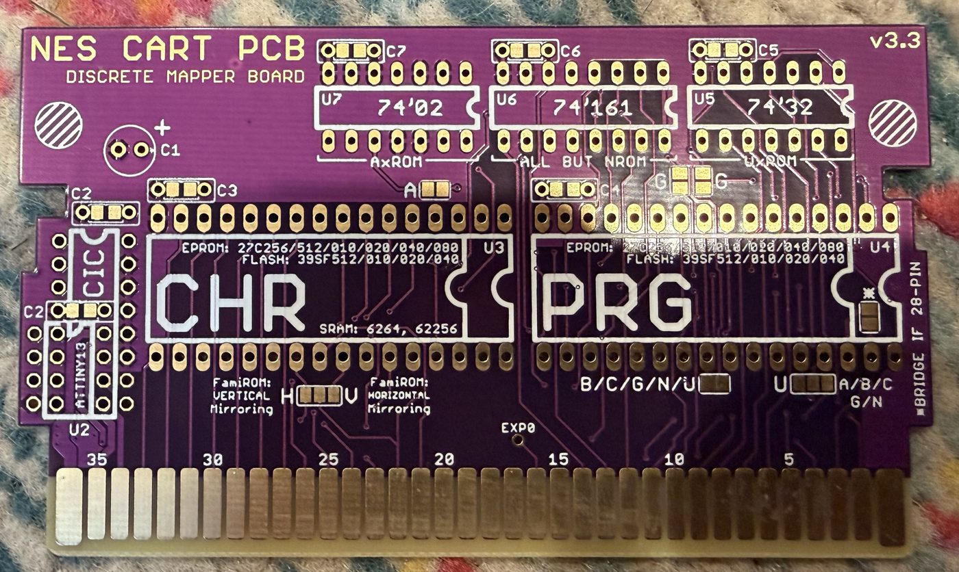
The board is the v3.3 discrete mapper board. Its letters are on its own back, in a legend: A is AxROM, B is BNROM, U is UxROM (the three with CHR RAM), C is CNROM, G is GNROM, N is NROM (the three with CHR ROM). The calibration ROM is NROM, so every jumper whose label carries an N is made, and every one whose label does not is left open. READ OFF THE SILKSCREEN 2026-09-30; not yet proven on the part. What proves it is the reader's dump.
| side | jumper, as labelled | for this cart |
|---|---|---|
| front | H, V (mirroring) | middle pad to H |
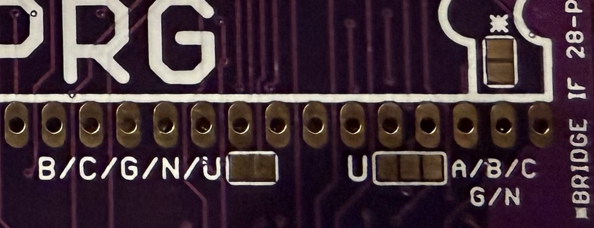
| front | B/C/G/N/U (two pads) | bridge |
| front | U against A/B/C G/N (three pads) | middle pad to the A/B/C G/N side |
| front | BRIDGE IF 28-PIN (two pads inside U4's outline, starred) | open: the chip has 32 pins |
| front | A (two pads, above CHR) | open |
| front | G, G (four pads, above PRG) | open |
| front | EXP0 | open |
| back | C/G/N against A/B/U, two columns of three pads | middle pad to the C/G/N side, on both columns |
| back | C/G, A/B, U (two blocks of three two-pad jumpers) | open, all six |
| back | A/B against U (the block by the CHR rows) | open |
| back | A (two pads by pin 32) | open |
| back | R0 to R7 | leave the traces as they are |
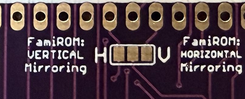
The mirroring letters are backwards, and the board says so in
words. cal.nes has vertical mirroring. The pad marked H has
"VERTICAL Mirroring" printed beside it and the pad marked V has
"HORIZONTAL Mirroring", and the board's guide admits it: "Solder the
middle pad to either H (for vertical mirroring) or V (for horizontal
mirroring). Yes, I know it's backwards". So it is H, by the words and
not by the letter. The picture never scrolls and uses one nametable, so
the wrong pad would show the same screens; the board and the file
should agree anyway.
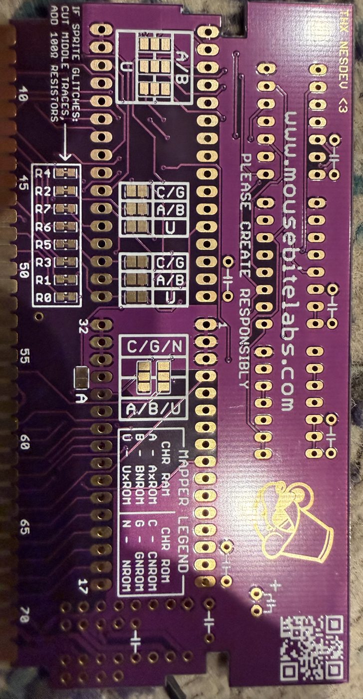
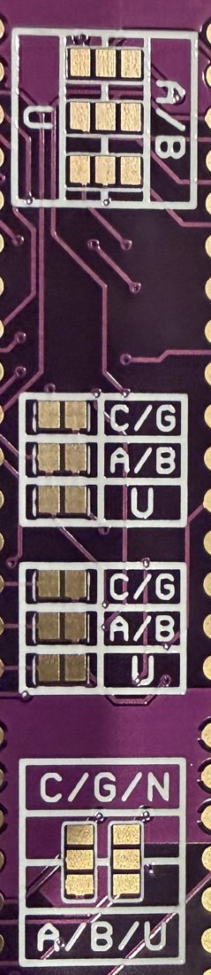
The close-up runs down the back between the ROM rows: the A/B against U block, the two blocks of C/G, A/B and U, and at the bottom the one that matters here, C/G/N over A/B/U, whose two columns each get their middle pad joined to the upper one.
On the back, the resistor positions R0 to R7 carry a note: if sprites glitch, cut the middle traces and add 100 ohm resistors. That is a repair for a fault not yet seen, so nothing is cut.
The parts the board takes for this cart
From the board's guide (https://mousebitelabs.com/2020/09/11/nes-reproduction-quick-guide-custom-pcb/) and its silkscreen. The values are the guide's; none has been measured.
| position | part | for this cart |
|---|---|---|
| U4 | SST39SF040 carrying prg.bin | fit: chip 1 |
| U3 | SST39SF040 carrying chr.bin | fit: chip 2 |
| C1 | about 22 uF electrolytic, 10 V or more, polarised (the + is marked) | fit |
| C3, C4 | about 0.1 uF ceramic, 10 V or more, one beside each ROM | fit |
| C2 | about 0.1 uF ceramic, beside the lockout chip's position | fit, or leave with U2 |
| U2 | the lockout chip (a CIC, or an ATtiny13 programmed as one) | empty: the console's lockout is defeated |
| U5, U6, U7 | 74'32, 74'161, 74'02 | empty: marked for UxROM, "all but NROM" and AxROM |
| C5, C6, C7 | their capacitors | empty with them |
The capacitors are not in the pile photographed on the day; they come from stock. A pair of 32-pin sockets at U3 and U4 would let a chip go back to the programmer when the ROM is revised; whether a socketed chip clears the shell has not been checked.
The rest of the pile is for other builds
| item | marking | what it is | where it belongs |
|---|---|---|---|
| Mapper 30 board | NES CART PCB (MAPPER 30) v1.2 | a flash and CHR RAM board | not this cart (cart-blanks.md) |
| SxROM board | NES CART PCB (SxROM) v3.1 | an MMC1 game board with save RAM | not this cart (cart-blanks.md) |
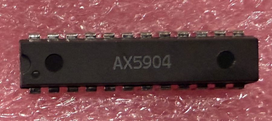
| 24-pin chip | AX5904 | the part the SxROM board names at its mapper position, beside MMC1 | the SxROM board's U5 |
| Black adapter | TL866, mousebitelabs v3.2 | seats 40 and 42-pin EPROMs in the programmer | not needed: a 32-pin chip sits in the programmer's own socket |
| Green adapter | NES CARTRIDGE ROM ADAPTER, NES MASK ROM | carries a 27C or 39SF part into a mask ROM's position on an original board | a donor-board build, not this one |
| 40-pin chip | WDC W65C02S6TPG-14 | a CMOS 6502 processor | not an NES part; a 65C02 computer's |
| 40-pin chip | WDC W65C22S6TPG-14 | a 65C22 interface adapter: two ports and two timers | the same computer's |
| 28-pin chip | CY62256NL-70PC | 32 KiB of static RAM, 70 ns | the CHR position of a CHR RAM board (both purple boards list 62256 there); not this cart, whose tiles are ROM |
| 14-pin chip | SN74LS00N | four two-input NAND gates | none of these boards: the discrete board takes '02, '161 and '32 |
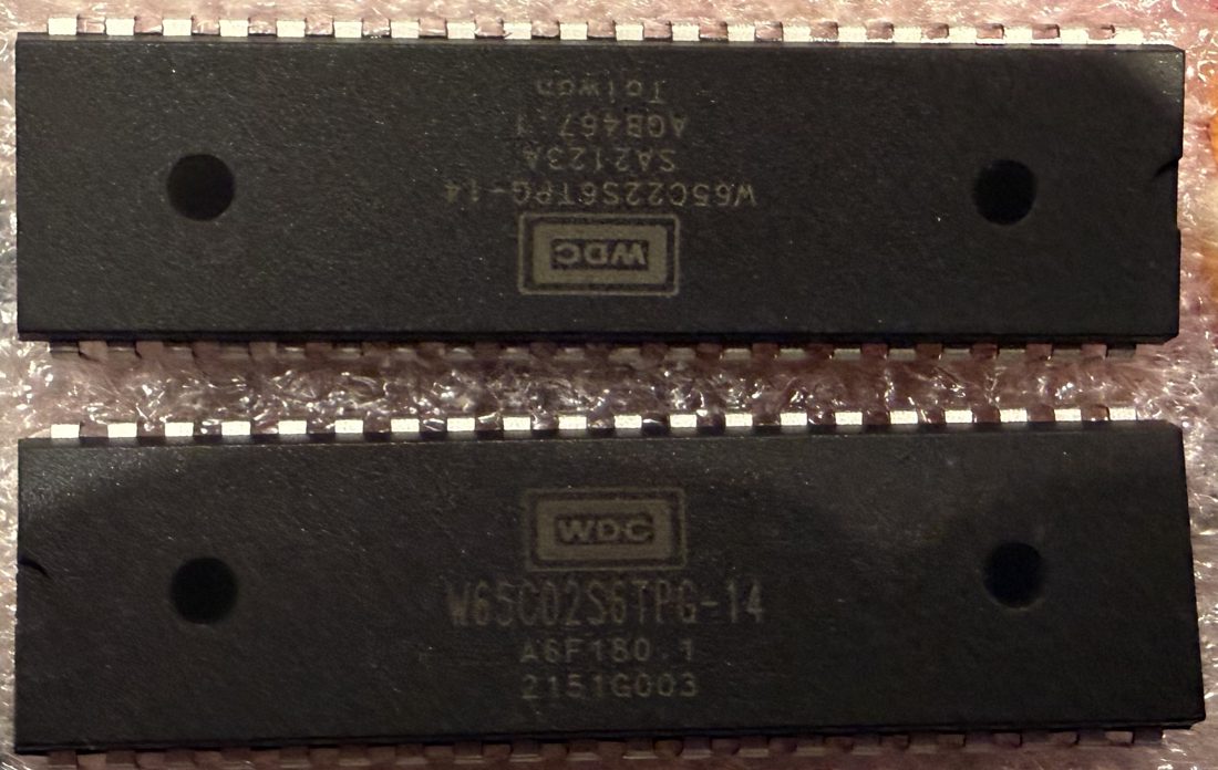
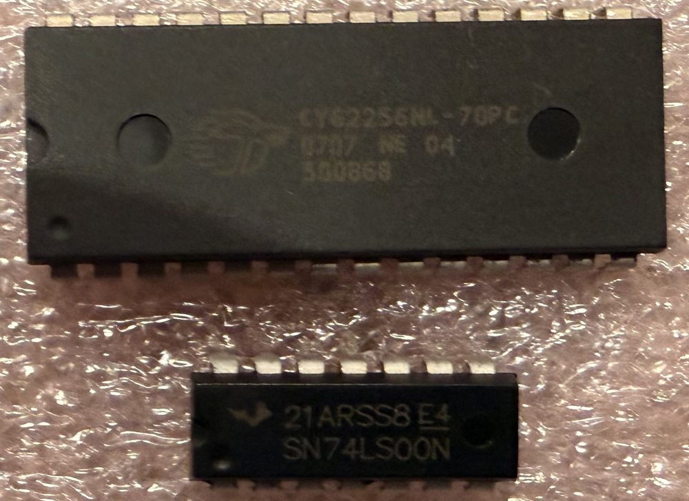
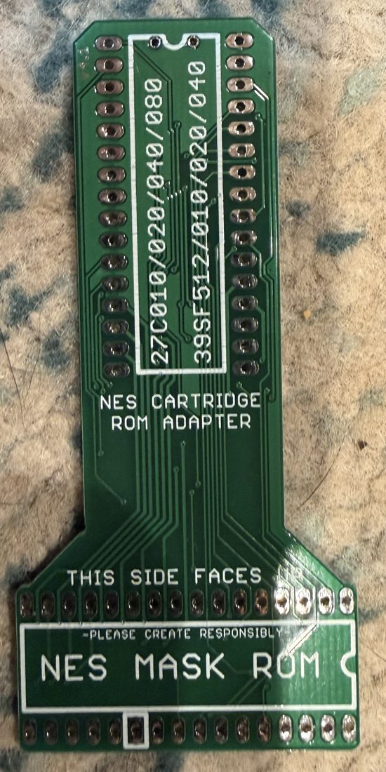
The processor, the interface adapter, the RAM and the NAND are the usual set for a breadboard 65C02 computer (a reading of the pile, not something anyone said). The W65C02 is the CMOS part and not the NMOS 6502 whose die the simulator runs.
What is open
- The five bridges, the capacitors, the two chips on the board.
- The reader's dump of the finished cart, whose body crc32 must be
21091B99. It is also what proves the jumper table above. - The cart in the console, and the strip read off a grabbed frame.
Pulled at build time from nes-bench/docs/cal-cart-build.md; the repository is the one copy. The reports use some working words of their own: Words the reports use.