The blank boards and the programmer
Photographed 2026-09-13 on the bench, the day the calibration ROM was
built and before its chips arrived. What each board is, read off its
own silkscreen, and what it means for cal.nes: an NROM image, 32 KiB
of program and 8 KiB of tiles (build-the-cal-cart.md). Nothing here
has been soldered or programmed yet; that is the open half of C0 in
calibration-plan.md.
The discrete mapper boards, and a mapper 30 board
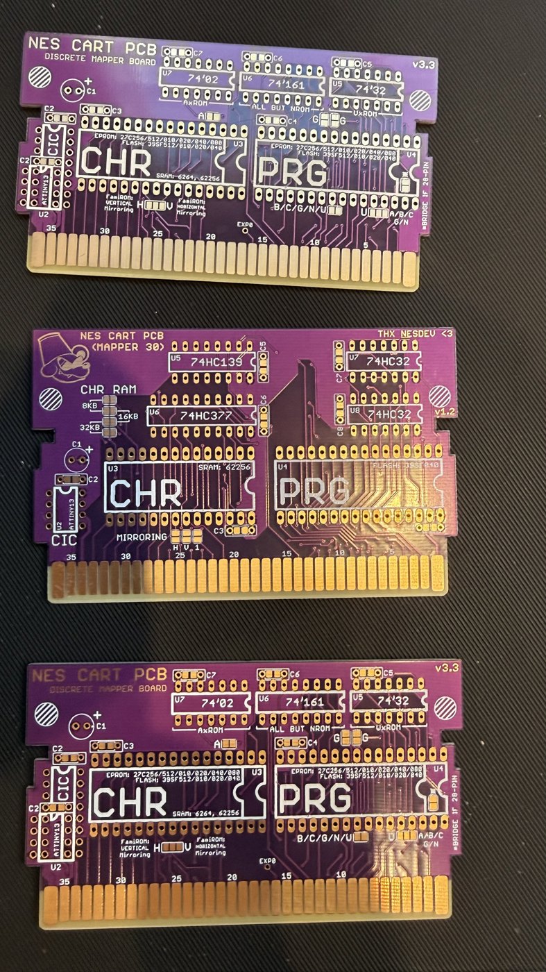
Two copies of a board marked NES CART PCB, DISCRETE MAPPER BOARD, v3.3:
footprints for a CHR ROM and a PRG ROM, a CIC, three logic parts
(74'02, 74'161, 74'32) whose rows are marked for which mapper they
serve (AxROM, UxROM, "all but NROM"), a mirroring jumper marked H and
V, and a row of letters (B, C, G, N, U) for the mapper families the
board takes. For the calibration cart this is the board (the owner's build spec,
2026-09-14): NROM needs no logic part fitted, so U5 to U7 stay
empty; the two ROM positions are U3 for CHR and U4 for PRG, each an
SST39SF040 (512 KiB of 5 V parallel flash) with the image tiled to fill
it (tools/nesprep.py, the tutorial's section 8); the console's
lockout is defeated, so the CIC position U2 stays empty; the H/V
jumper follows the file's mirroring bit, vertical, which on this board
is the pad marked H (its letters are backwards and its words are not:
cal-cart-build.md, which also has every other jumper, both sides).
Between them a board marked NES CART PCB, MAPPER 30, v1.2, with 74HC139, 74HC377 and 74HC32 and a CHR RAM footprint marked 8 KB, 16 KB and 32 KB. Not for this ROM: mapper 30 is a flash-and-CHR-RAM board.
An SxROM board
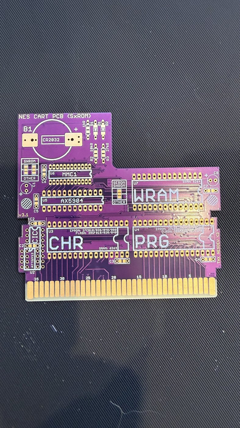
NES CART PCB (SxROM), v3.1: an MMC1 position marked MMC1 and AX5904, a WRAM footprint, a CR2032 holder for the save RAM, CHR and PRG ROMs and a CIC. A game board, not a test board; the calibration ROM would need its mapper registers written, which it does not do.
The EPROM adapter for the programmer
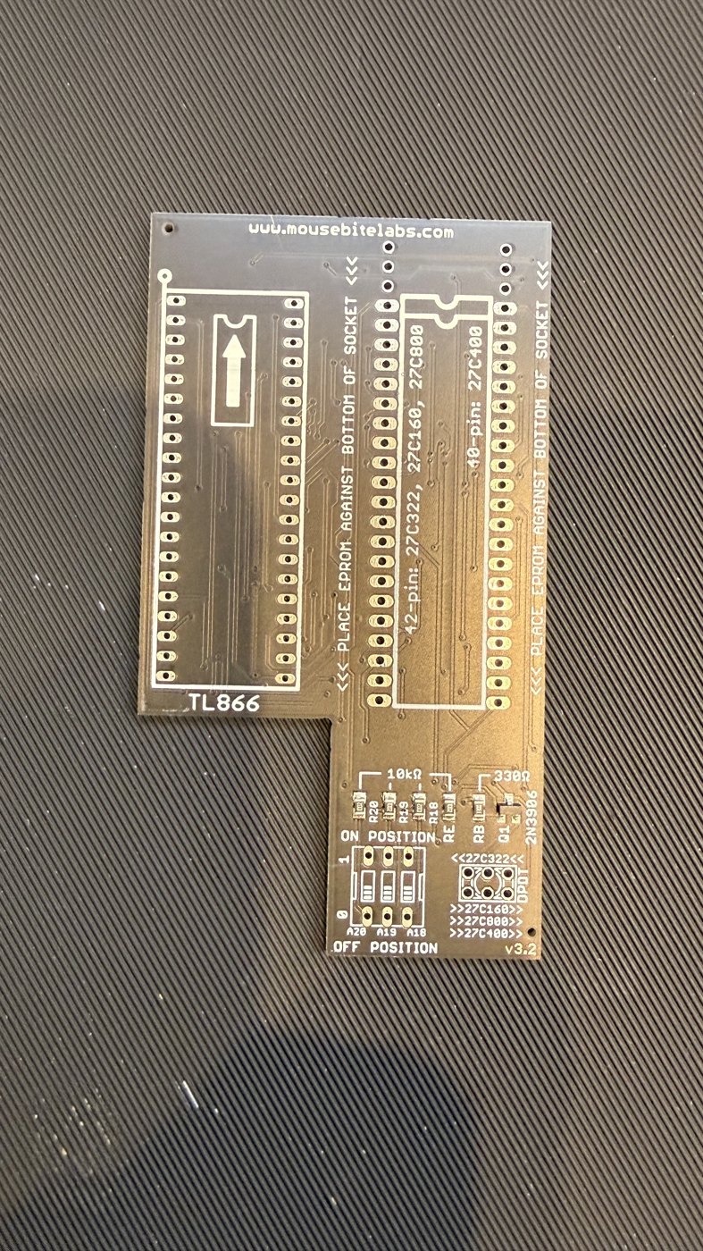
An adapter from mousebitelabs.com, v3.2, that sits in a TL866-class programmer's socket and takes 42-pin (27C322, 27C160, 27C800) and 40-pin (27C400) EPROMs, with the instruction to place the EPROM against the bottom of the socket, and switches for A20, A19 and A18 marked with their ON and OFF positions. Those are large parts for banked boards; the SST39SF040s this cart uses are 32-pin DIPs that sit in the programmer's own socket without the adapter.
The programmer
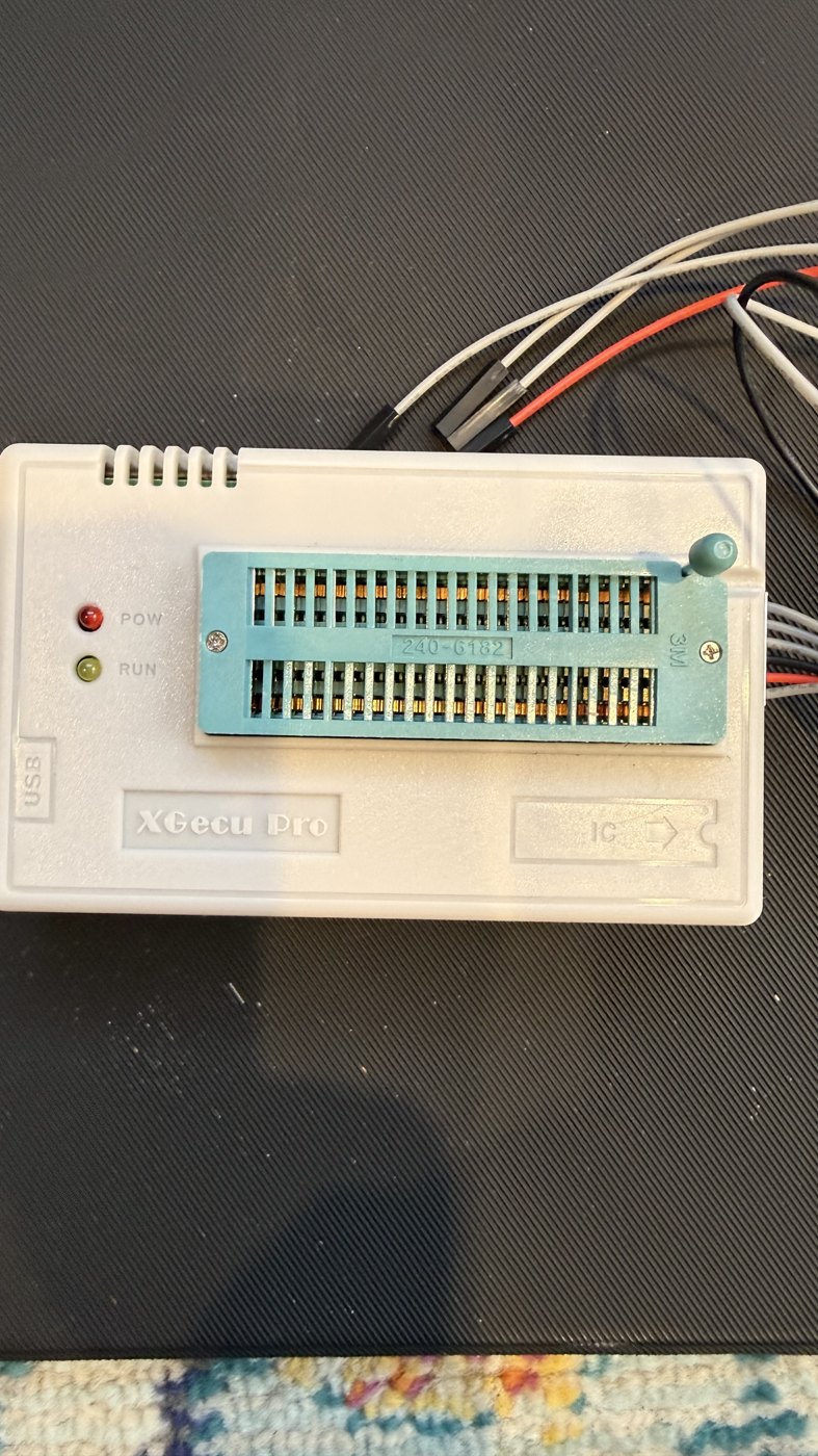
An XGecu Pro (the TL866 family; it enumerates as a TL866II Plus,
MEASURED 2026-09-30) with a 40-pin ZIF socket, its USB lead
and the two jumper wires that came with it. This is what writes the
two images tools/nesprep.py makes from cal.nes into the ROMs.
What is not known yet
- The chips themselves: on the bench 2026-09-30, and the first one
written that evening. The build from there is
cal-cart-build.md, which also names the parts photographed since. - The reader's dump of the finished cart, whose body crc32 must be
21091B99(MEASURED 2026-09-13 on the exported file).
Pulled at build time from nes-bench/docs/cart-blanks.md; the repository is the one copy. The reports use some working words of their own: Words the reports use.